Thin film transistor, array substrate and display panel

A thin film transistor, oxide semiconductor technology, applied in transistors, semiconductor devices, electric solid devices, etc., can solve the problems of TFT stability decline, affecting display effect, etc., and achieve the effect of improving stability

Active Publication Date: 2017-06-27
SHANGHAI TIANMA MICRO ELECTRONICS CO LTD
View PDF4 Cites 1 Cited by
  • Summary
  • Abstract
  • Description
  • Claims
  • Application Information

AI Technical Summary

Problems solved by technology

However, since the oxide semiconductor is more sensitive to blue-violet light in the visible light band, when the blue-violet light provided by the backlight enters the active layer of the TFT, the stability of the TFT decreases, which affects the display effect.

Method used


Image

  • Thin film transistor, array substrate and display panel
  • Thin film transistor, array substrate and display panel
  • Thin film transistor, array substrate and display panel

Examples


Embodiment Construction

[0017] The application will be further described in detail below in conjunction with the accompanying drawings and embodiments. It should be understood that the specific embodiments described here are only used to explain related inventions, rather than to limit the invention. It should also be noted that, for the convenience of description, only the parts related to the related invention are shown in the drawings.

[0018] It should be noted that, in the case of no conflict, the embodiments in the present application and the features in the embodiments can be combined with each other. The present application will be described in detail below with reference to the accompanying drawings and embodiments.

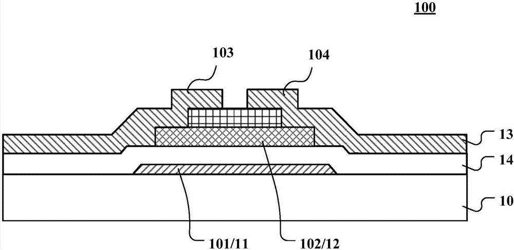
[0019] Please refer to figure 1 , which shows a schematic structural view of an embodiment of a thin film transistor according to the present application.

[0020] Such as figure 1 As shown, the thin film transistor 100 includes a gate 101 , an active layer 102 , a source ...


PUM

PropertyMeasurementUnit
thicknessaaaaaaaaaa
thicknessaaaaaaaaaa

Abstract

The application discloses a thin film transistor, array substrate and display panel. A specific embodiment of the thin film transistor includes a gate, an active layer, a source electrode and a drain electrode; the gate is formed on a gate metal layer, the active layer is formed on an oxide semiconductor layer, the source electrode and the drain electrode are formed on a source and drain metal layer, the source and drain metal layer is located at one side of the oxide semiconductor layer away from the gate metal layer, and the source electrode and the drain electrode are in contact with the active layer; a gate insulation layer is arranged between the gate and the active layer; and transmittance of the gate insulation layer to light of any wavelength lambda1 is lower than that to light with any wavelength lambda2, wherein 400nm<=lambda1<=480nm, and 480nm<=lambda2<=780nm. By adoption of the scheme of the application, the stability of the thin film transistor can be improved.

Description

technical field [0001] The present application relates to the field of display technology, in particular to thin film transistors, array substrates and display panels. Background technique [0002] A TFT (Thin Film Transistor, thin film transistor) liquid crystal display has the advantages of high brightness, low power consumption, long life, etc., and is widely used in the display field. TFTs generally include an active layer for supplying carriers. When the gate of the TFT receives a voltage signal, carriers migrate in the channel of the active layer. [0003] An existing TFT uses an oxide semiconductor (such as indium gallium zinc oxide) as an active layer material, and this material has relatively high carrier mobility. However, since oxide semiconductors are more sensitive to blue-violet light in the visible light band, when the blue-violet light provided by the backlight enters the active layer of the TFT, the stability of the TFT decreases, thereby affecting the dis...

Claims


Application Information

Patent Timeline
Patent Type & Authority Applications(China)
IPC IPC(8): H01L29/786H01L29/423H01L29/51H01L27/12G02F1/1368
Inventor 应变符鞠建何泽尚
Owner SHANGHAI TIANMA MICRO ELECTRONICS CO LTD
Why Eureka
Try Eureka