GaN-based light emitting diode epitaxial wafer and manufacturing method therefor

A technology of light-emitting diodes and manufacturing methods, which is applied in the direction of electrical components, circuits, semiconductor devices, etc., can solve the problems of narrow growth window and limited effect of InGaN stress release layer, and achieve the goal of increasing lateral expansion capability, reducing stress, and improving photoelectric performance Effect

Active Publication Date: 2017-06-30
HC SEMITEK ZHEJIANG CO LTD
View PDF4 Cites 8 Cited by
  • Summary
  • Abstract
  • Description
  • Claims
  • Application Information

AI Technical Summary

Problems solved by technology

[0005] In order to solve the problem that the existing current spreading layer will cause the growth window of the InGaN stress release layer directly grown later to be very narrow, and it

Method used


Image

  • GaN-based light emitting diode epitaxial wafer and manufacturing method therefor
  • GaN-based light emitting diode epitaxial wafer and manufacturing method therefor
  • GaN-based light emitting diode epitaxial wafer and manufacturing method therefor

Examples


Example Embodiment

[0027] In order to make the objectives, technical solutions, and advantages of the present invention clearer, the embodiments of the present invention will be described in further detail below in conjunction with the accompanying drawings.

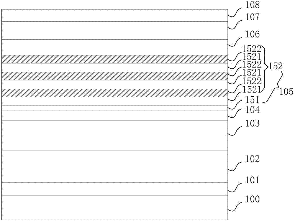
[0028] figure 1 It is a schematic structural diagram of a GaN-based light-emitting diode epitaxial wafer provided by an embodiment of the present invention, see figure 1 , The GaN-based light-emitting diode epitaxial wafer includes: a substrate 100, a buffer layer 101, a three-dimensional growth layer 102, a u-GaN layer 103, an n-type layer 104, an n-type current spreading layer 105, a stress The release layer 106, the multiple quantum well layer 107 and the p-type layer 108. The n-type current spreading layer 105 includes a first sub-layer 151 covering the n-type layer 104 and a second sub-layer 152 covering the first sub-layer 151 , The first sublayer 151 is an AlGaN layer, the second sublayer 152 is a superlattice structure formed by a GaN ...


PUM

PropertyMeasurementUnit
Thicknessaaaaaaaaaa

Abstract

The invention discloses a GaN-based light emitting diode epitaxial wafer and a manufacturing method therefor and belongs to the field of light emitting diodes. The GaN-based light emitting diode epitaxial wafer comprises a substrate, a buffer layer, a three-dimensional growth layer, a u-GaN layer, an n type layer, an n type current expansion layer, a stress releasing layer, a multiple quantum well layer and a p type layer; wherein the buffer layer, the three-dimensional growth layer, the u-GaN layer, the n type layer, the n type current expansion layer, the stress releasing layer, the multiple quantum well layer and the p type layer orderly arranged on the substrate in a covering manner; the n type current expansion layer comprises a first sub-layer covering the n type layer and a second sub-layer covering the first sub-layer; the first sub-layer is an AlGaN layer, the second sub-layer is of a superlattice structure formed by a non-Si-doped GaN layer and an Si-doped GaN layer, the first sub-layer is higher than the n type layer and the second sub-layer in terms of growth temperature, and the second sub-layer is greater than the first sub-layer in terms of growth pressure. The GaN-based light emitting diode epitaxial wafer is capable of overcoming defects and improving photoelectric performance.

Description

technical field [0001] The invention relates to the field of light-emitting diodes, in particular to a GaN-based light-emitting diode epitaxial wafer and a manufacturing method thereof. Background technique [0002] As a hot spot that people have been paying attention to, GaN materials are widely used in light emitting diodes (English: Light Emitting Diode, referred to as: LED) devices. The light emitting diodes developed with GaN are pure in color, high in brightness, and low in energy consumption. They are widely used in lighting, Medical, display, signal, toys and many other fields. [0003] However, with the continuous expansion of the application range of LEDs, people have higher requirements for the new generation of LEDs. In order to meet the needs of customers, LEDs need to have higher light efficiency and stronger antistatic ability. Generally, LEDs with stronger antistatic ability will show better electrical stability during use, and LEDs with higher light efficie...

Claims


Application Information

Patent Timeline
IPC IPC(8): H01L33/02H01L33/04H01L33/14H01L33/00
Inventor 李红丽胡加辉
Owner HC SEMITEK ZHEJIANG CO LTD
Why Eureka
Try Eureka