

Dielectric waveguide coupling structure and multi-stage dielectric waveguide filter
A technology of dielectric waveguide and coupling structure, used in waveguide-type devices, electrical components, circuits, etc., can solve the problems of limited length/coupling amount, large volume of multi-order filters, etc., which is conducive to miniaturized design and simplified processing process , the effect of reducing the volume
- Summary
- Abstract
- Description
- Claims
- Application Information
AI Technical Summary
Problems solved by technology
Method used
Image

Examples
Embodiment 1
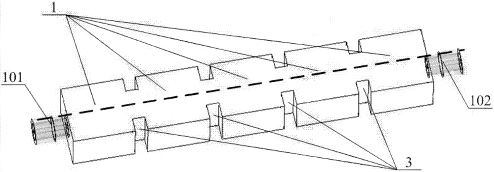
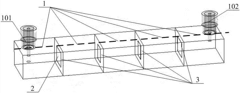
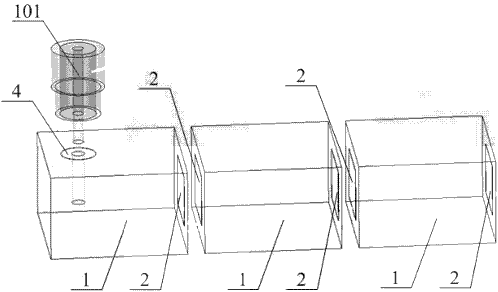
[0028] figure 2 It shows a schematic structural diagram of the first multi-order dielectric waveguide filter provided by the present invention, image 3 It shows a schematic diagram of the large partial split structure in the first multi-order dielectric waveguide filter provided by the present invention, Figure 4 It shows a schematic diagram of the small partial split structure in the first multi-order dielectric waveguide filter provided by the present invention.
[0029] This embodiment provides a fifth-order dielectric waveguide filter with a linear structure, including a first waveguide joint 101, a second waveguide joint 102, and five dielectric waveguide monomers 1 sequentially connected in series to form a waveguide main channel, wherein the The first waveguide joint 101 and the second waveguide joint 102 are respectively connected to the dielectric waveguide monomers 1 located at both ends of the main waveguide channel; the two adjacent dielectric waveguide monomer...
Embodiment 2
[0038] Figure 5 A schematic structural diagram of the second multi-order dielectric waveguide filter provided by the present invention is shown. This embodiment still provides a fifth-order dielectric waveguide filter, which differs from the fifth-order dielectric waveguide filter described in Embodiment 1 in that: the fifth-order dielectric waveguide filter has a Z-shaped structure, that is, The waveguide main channel of the fifth-order dielectric waveguide filter is a "Z"-shaped channel. Therefore, the filter can be three-dimensional, and the volume of the device can be further reduced. In addition, the main channel of the waveguide may also be, but not limited to, a channel in the form of a "U"-shaped channel or the like.
[0039] The technical effect of the fifth-order dielectric waveguide filter provided in this embodiment is based on the technical effect of the first embodiment, and further includes the following: (1) The filter can be three-dimensional, and the volum...
Embodiment 3
[0040] Figure 6 A schematic structural diagram of the third multi-order dielectric waveguide filter provided by the present invention is shown. This embodiment provides a multi-order dielectric waveguide filter with a hybrid coupling structure, which includes two inductive through-hole coupling structures 5 with frequency-adjusting blind holes 501, and allows the two parts of the inductive through-hole coupling structure 5 to pass through The dielectric waveguide coupling structure described in Embodiment 1 is combined to form a three-dimensional filter structure overlapping up and down, further reducing the volume of the device.
[0041] The technical effect of the multi-order dielectric waveguide filter provided in this embodiment can be easily derived by referring to the technical effect of the second embodiment, and will not be repeated here.
PUM
 Abstract
Description
Claims
Application Information