A plasma processing device and method for uniformly etching a substrate

A plasma and processing device technology, which is applied in the fields of semiconductor processing and ion distribution, and can solve the problems of uneven etching rate in the central area and edge area of ​​the substrate, consumption of the surface of the focus ring by etching, and reduction of the height of the focus ring surface. , to achieve the effect of ensuring etching uniformity, increasing thickness and prolonging service life

Active Publication Date: 2019-05-31
ADVANCED MICRO FAB EQUIP INC CHINA
View PDF5 Cites 0 Cited by
  • Summary
  • Abstract
  • Description
  • Claims
  • Application Information

AI Technical Summary

Problems solved by technology

The existing technology uses silicon or silicon carbide as the base material to make the focus ring. With the extension of the etching process time, the surface of the focus ring will also be consumed by plasma etching.
The surface height of the focus ring decreases, the plasma sheath above it moves down, and the etching process in the edge area of ​​the substrate changes, resulting in uneven etching rates in the center area and edge area of ​​the substrate

Method used


Image

  • A plasma processing device and method for uniformly etching a substrate
  • A plasma processing device and method for uniformly etching a substrate
  • A plasma processing device and method for uniformly etching a substrate

Examples


Embodiment Construction

[0038] The technical solution of the present invention will be described in detail below in conjunction with the accompanying drawings.

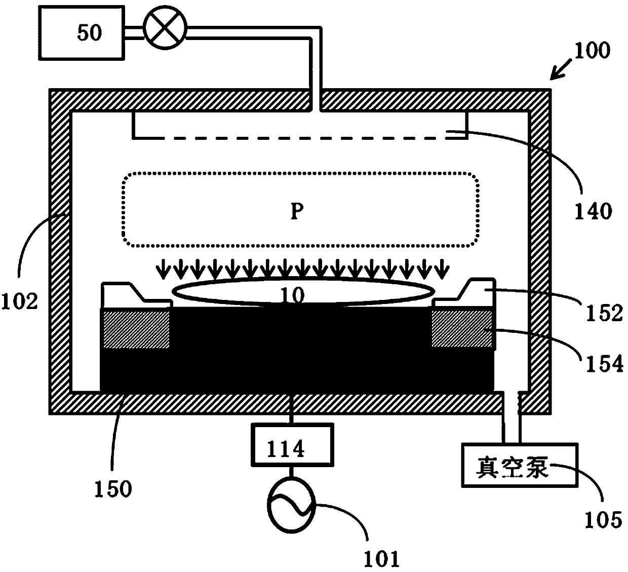
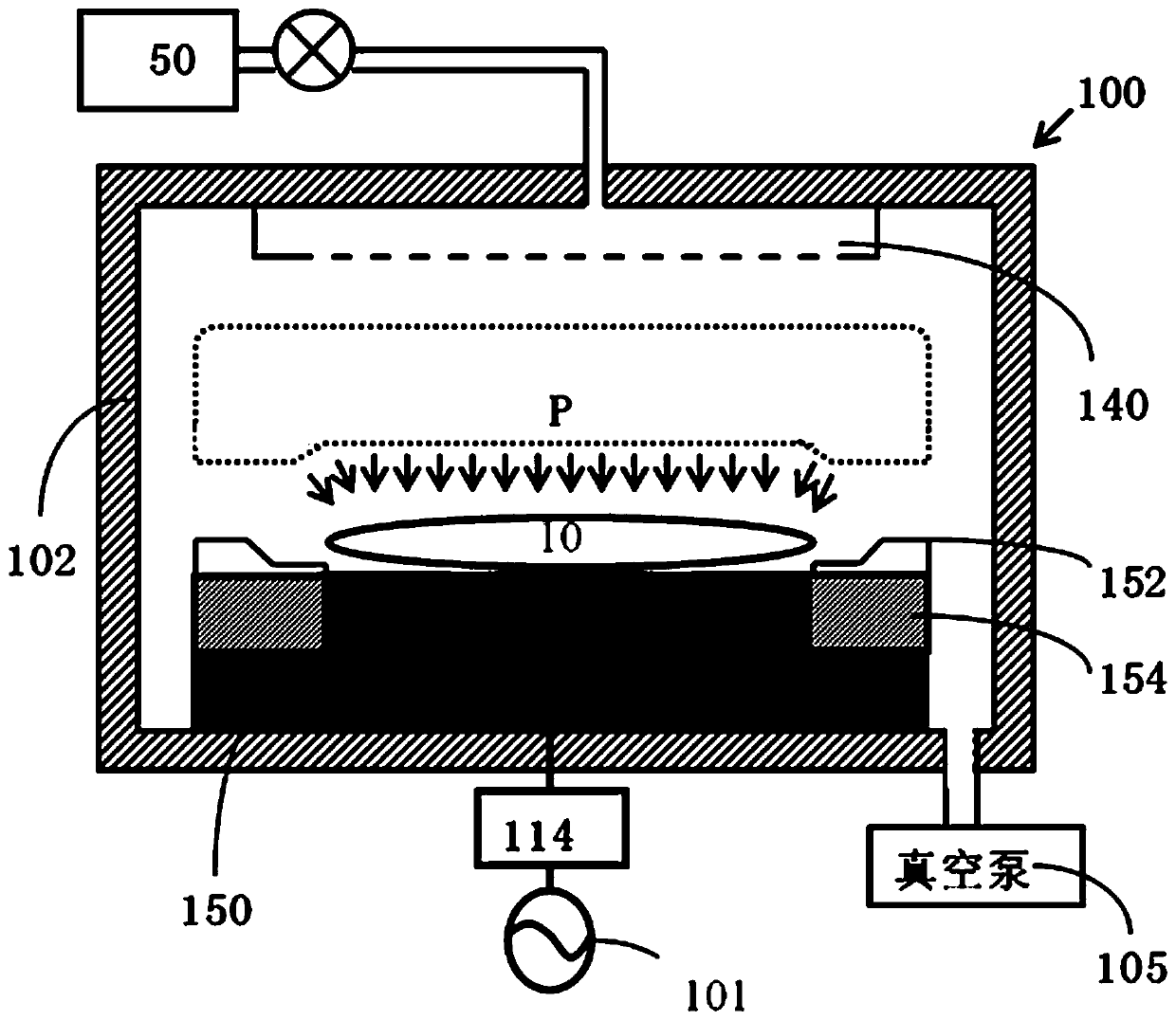
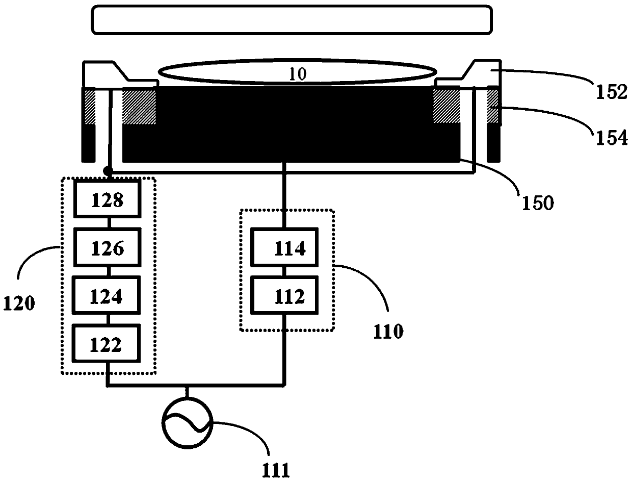
[0039] figure 1 A schematic structural view of a plasma processing device is shown. As shown in the figure, the plasma processing device includes a processing chamber 100, the processing chamber 100 is substantially cylindrical, and includes a vertical reaction chamber side wall 102, The processing chamber 100 has an upper electrode 140 and a lower electrode 150 arranged parallel to each other. The upper electrode 140 is connected with the reaction gas source 50, and the gas in the reaction gas source 50 is evenly injected into the inside of the reaction chamber through the upper electrode 140; A high radio frequency energy field is formed between them to form a processing area P that ignites and maintains the plasma, in which the reactive gas can be dissociated into the plasma required for the process. The lower electrode 150, also known ...


PUM


Abstract

The invention discloses a plasma processing device and method of a uniform etching substrate. The plasma processing device comprises a plasma processing cavity, wherein a base is arranged in the plasma processing cavity and is used for supporting the substrate, a focusing ring encircles the substrate, at least two automatic bias voltages which can be superimposed are generated on a surface of the focusing ring by applying a radio frequency signal, and when the thickness of the focusing ring is corroded and thinned with plasma bombarding, the phase of a certain automatic bias voltage is adjusted so that phase difference exists between the two automatic bias voltages. and therefore the sum of the automatic bias voltages after being superimposed is changed, and the regulation of plasma distribution of an edge region of the substrate is achieved.

Description

technical field [0001] The invention relates to the technical field of semiconductor processing, in particular to a technical field capable of uniformly adjusting plasma distribution in the edge region of a substrate. Background technique [0002] In a plasma processing device, in order to ensure uniform distribution of electric field lines in the center and edge regions of the substrate, it is usually necessary to set a focus ring around the substrate, which can extend the distribution edge of the plasma above the substrate to the focus The outer edge of the ring widens the density profile of the plasma on the substrate surface. The density distribution of the plasma in the edge area on the surface of the substrate tends to be gentle, and the plasma distribution in the central area and the edge area of ​​the substrate is more uniform, thereby realizing the uniformity of substrate etching. [0003] The focus ring is a component that has a significant impact on the edge etch...

Claims


Application Information

Patent Timeline
Patent Type & Authority Patents(China)
IPC IPC(8): H01J37/32
CPCH01J37/32082H01J37/32174H01J37/32183H01J37/32642
Inventor 梁洁杨平
Owner ADVANCED MICRO FAB EQUIP INC CHINA
Why Eureka
Try Eureka