
High-power eutectic solder inversion structure for ultraviolet LED chip

A LED chip, high-power technology, applied in the direction of electrical components, electric solid devices, circuits, etc., can solve problems affecting stability, heat dissipation, and service life, so as to improve the light output rate and service life, increase the light output rate, and improve The effect of light output

Active Publication Date: 2017-07-04
GUANGDONG UNIV OF TECH
View PDF6 Cites 3 Cited by
  • Summary
  • Abstract
  • Description
  • Claims
  • Application Information

AI Technical Summary

Problems solved by technology

However, the distance between the encapsulant and the chip is relatively close, and the heat released during the working process of the chip is not easily dissipated by the encapsulant with poor thermal conductivity, and the heat radiation effect is still strong. Effective heat exchange affects its stability, heat dissipation and service life, so the existing UV LED flip-chip structure needs to be further improved and perfected

Method used


Image

  • High-power eutectic solder inversion structure for ultraviolet LED chip
  • High-power eutectic solder inversion structure for ultraviolet LED chip
  • High-power eutectic solder inversion structure for ultraviolet LED chip

Examples


Embodiment 1

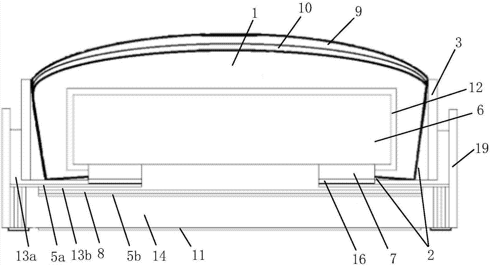
[0051] like figure 1 As shown, the present invention discloses a high-power ultraviolet LED chip eutectic soldering flip-chip structure, which mainly includes an ultraviolet LED chip 6, a packaging adhesive layer 1, a reflective cup 2, a first copper layer 5a, a welding pad 7, and a lens 9. An anti-reflection film 10 and a silicone layer 12 . The LED chip 6 is sequentially welded on the first copper layer 5 a through the pad 7 and the conductive and thermally conductive adhesive layer 16 , and the two copper layers are separated and insulated from each other. The right triangle reflective cup 2 is fixed on the first copper layer 5a through the first thermally conductive adhesive layer 13a, and is connected with the first copper layer 5a. The reflective cup 2 is used to reflect part of the ultraviolet light emitted from the LED chip 6 to the side and to fix the packaging form of the LED.

[0052] Among them, the production of the micro PCB substrate uses a mold to grow the s...

Embodiment approach

[0076] In addition, the heat dissipation structure of the miniature PCB substrate also has another embodiment: the middle part of the miniature PCB substrate 4 is provided with a slot for accelerating heat dissipation, and the slot extends from the upper surface layer of the substrate to the lower surface layer and runs through the entire surface. block substrate. The second thermally conductive adhesive layer 13b extends into the slot and fills up the slot, thereby forming a convex-convex structure, so that the heat generated by the LED chip 6 can be quickly dissipated from the bottom to obtain a better heat dissipation effect.

[0077] Further, the positive and negative electrode strips at both ends of the micro PCB substrate 4 are composed of independent, parallel sub-electrode strips at a certain interval, and the electrode strips are used as a bridge connecting the inside of the LED chip 6 with the external circuit. The parallel connection of the sub-electrode strips ensu...


PUM


Abstract

The invention discloses a high-power eutectic solder inversion structure for an ultraviolet LED chip. The high-power eutectic solder inversion structure mainly comprises an LED chip, a silica gel layer, a packaging adhesive layer, a lens, an antireflection film, reflection cups, a miniature PCB substrate, copper layers, conductive and heat-conducting adhesive layers and bonding pads, wherein the PCB substrate comprises an upper surface layer, a middle layer and a lower surface layer; a groove is arranged in the middle of the upper surface layer of the substrate; and a second copper layer, an SiC layer and a second heat-conducting adhesive layer are sequentially arranged in the groove from bottom to top. Better light transmission and heat dissipation effects are obtained through improving the order of various layers of the substrate and the interlayer structures, and meanwhile, the halo phenomenon is avoided to the maximum extent. Electrode strips are also arranged at two ends of the substrate, and meanwhile, the structure of the miniature PCB substrate is improved, thereby assisting the chip in dissipating heat; and a solid heat emission hole filled with copper is arranged between the upper surface layer and the lower surface layer, thereby accelerating heat loss. The high-power eutectic solder inversion structure also has the advantages of being reasonable in structure, low in technological requirements, easy to produce, high in yield and high in light extracting rate.

Description

technical field [0001] The invention relates to the field of LED packaging structures, in particular to a high-power ultraviolet LED chip flip-chip structure in which an LED chip is fixed on a PCB substrate through a flip-chip process. Background technique [0002] Ultraviolet LED products have the advantages of energy saving, environmental protection, power saving, high efficiency, fast response, long service life, high reliability and no mercury, so the ultraviolet LED industry has attracted much attention in recent years. Specific applications of UV LED products include: UV LED induction lamps, faucet purifiers, UV LED fishing lamps, UV LED medical treatments, etc. [0003] Some ultraviolet LED chip flip-chip packaging methods in the prior art, the flip chip is solidified on the substrate through electrodes, solder, conductive wiring layers, etc., and then the packaging glue is injected and filled through a mold such as a lens, and the mold tops to the substrate. The LED...

Claims


Application Information

Patent Timeline
Patent Type & Authority Applications(China)
IPC IPC(8): H01L33/48H01L33/58H01L33/62H01L33/64
CPCH01L33/486H01L33/58H01L33/62H01L33/641H01L33/642H01L33/647H01L2224/14H01L2224/16225
Inventor 何苗杨思攀熊德平王成民
Owner GUANGDONG UNIV OF TECH
Learn More