Column-level ADCs for cmos image sensors with hybrid CDs

An image sensor and column-level technology, applied in the field of column-level ADC, can solve the problem of reducing the quantization speed of ADC, and achieve the effect of reducing the impact and improving the quantization speed

Active Publication Date: 2020-01-17
天津海芯光电科技有限公司
View PDF5 Cites 0 Cited by
  • Summary
  • Abstract
  • Description
  • Claims
  • Application Information

AI Technical Summary

Problems solved by technology

[0003] However, in the ADC using digital CDS, due to the two quantizations of the reset signal and the exposure signal of the pixel, and then the quantized digital code value is differenced to eliminate some non-ideal factors at the column level, which will greatly reduce the ADC quantization speed

Method used


Image

  • Column-level ADCs for cmos image sensors with hybrid CDs
  • Column-level ADCs for cmos image sensors with hybrid CDs
  • Column-level ADCs for cmos image sensors with hybrid CDs

Examples


Embodiment Construction

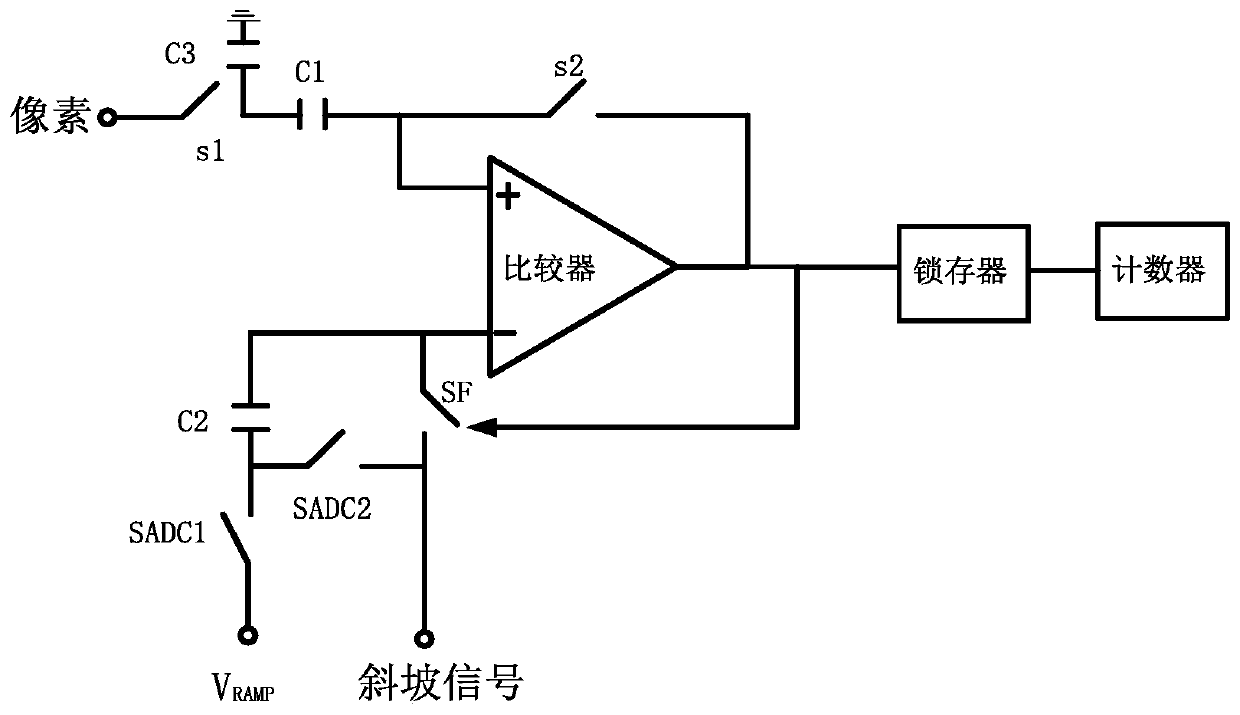
[0012] The technical scheme of the present invention is, adopt the block diagram of the two-step monoclinic rank ADC circuit structure of H-CDS as figure 2 . It includes comparators, latches, counters, capacitors C1, C2, C3 and switches SADC1, SADC2, S1, S2, and SF. The pixel output is connected to the upper plates of the capacitors C1 and C3 through the switch s1. The lower plate of capacitor C3 is grounded, and the lower plate of capacitor C1 is connected to the non-inverting input terminal of the comparator. Moreover, the non-inverting input terminal of the comparator is connected to the output terminal of the comparator through the switch s2. The inverting input terminal of the comparator is connected to the ramp signal through the switch SF, and at the same time, the inverting input terminal is connected to the reference voltage through the capacitor C2 and the switch SADC1. The upper plate of the capacitor C2 is connected to the inverting input terminal of the compar...


PUM


Abstract

The invention relates to the field of analog integrated circuit design of microelectronics. It proposes an implementation method of a two-step monoclinic ADC using H-CDS to meet the high-speed and low-noise requirements of a CMOS image sensor for a readout circuit. The technical solution adopted in the present invention is that the CMOS image sensor column-level ADC with hybrid CDS includes a comparator, a latch, a counter, capacitors C1, C2, C3 and switches SADC1, SADC2, S1, S2 and SF, and the pixel output Connect to the upper plate of capacitor C1 and capacitor C3 through switch s1, the lower plate of capacitor C3 is grounded, and the lower plate of capacitor C1 is connected to the non-inverting input terminal of the comparator; and, the non-inverting input terminal of the comparator is connected to the non-inverting input terminal through switch s2 The output terminals of the comparators are connected, and the inverting input terminal of the comparator is connected to the ramp signal through the switch SF. The invention is mainly applied to the occasion of designing analog integrated circuits of microelectronics.

Description

technical field [0001] The invention relates to the field of analog integrated circuit design of microelectronics, in particular to a column-level ADC used for mixing CDS in a CMOS image sensor. Background technique [0002] CMOS image sensors have been widely used in applications such as digital cameras, automotive security recorders, and medical equipment. The schematic diagram of the traditional CIS structure is as follows: figure 1 , usually including pixels, correlated double sampling (CDS), analog-to-digital converter (ADC) and some digital processing modules, etc. Among these modules, the ADC is an important module that converts the analog pixel voltage value into a digital value. From the classification of ADCs, there are chip-level ADCs, column-level ADCs, and pixel-level ADCs. Generally, column-level ADCs are widely used in consideration of comprehensive speed, chip area, and power consumption. However, since each column of ADCs cannot be completely identical, ...

Claims


Application Information

Patent Timeline
Patent Type & Authority Patents(China)
IPC IPC(8): H04N5/3745H04N5/378
CPCH04N25/772H04N25/75
Inventor 徐江涛徐爽韩立镪高静史再峰
Owner 天津海芯光电科技有限公司
Why Eureka
Try Eureka