LED illuminating device and manufacturing method thereof

A technology of LED lighting and LED chips, which is applied to lighting devices, components of lighting devices, lighting and heating equipment, etc. It can solve the problems of lack of advantages in LED chip bonding and welding processes, high mass production costs, and low process reliability. problems, to achieve the effect of reducing the amount of deformation, using less metal materials, and improving the manufacturing yield

Inactive Publication Date: 2017-07-07
LONGWIDE TECH
View PDF17 Cites 1 Cited by
  • Summary
  • Abstract
  • Description
  • Claims
  • Application Information

AI Technical Summary

Problems solved by technology

[0004] Chinese patent CN102494257A, a large-angle LED bulb with natural convection heat dissipation inside and outside the air. In this case, the LED chip is attached to a polygonal heat dissipation column with multiple heat dissipation channels, and the air naturally circulates through the heat dissipation channels to dissipate heat. The heat dissipation column can only provide lighting in the direction of the circular circumference, and the scheme of other lighting ranges has not been proposed;
[0018] In the known sheet metal process, stamping is extended into a 3D structure and then cut to form a circuit to form a conductive plate similar to the present invention, but such a process is relatively fast in forming a spatial structure, but it is difficult to cut the circuit and then use it manually. LED chip bonding and soldering processes on three-dimensional curved surfaces lack advantages, and such solutions are limited by high mass production costs and low process reliability.

Method used


Image

  • LED illuminating device and manufacturing method thereof
  • LED illuminating device and manufacturing method thereof
  • LED illuminating device and manufacturing method thereof

Examples


Embodiment Construction

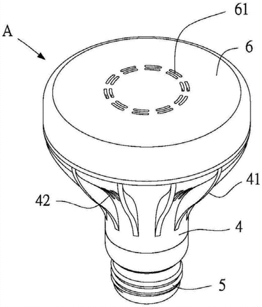
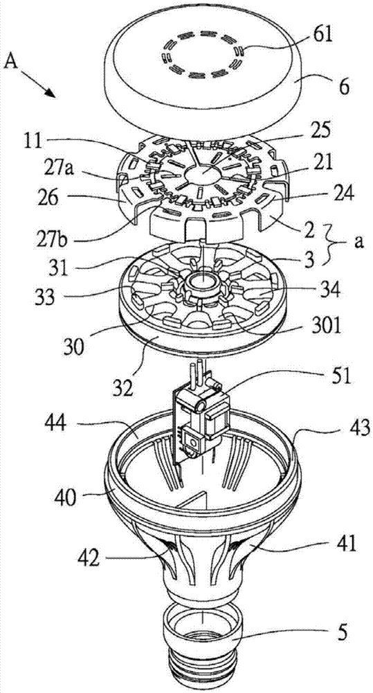
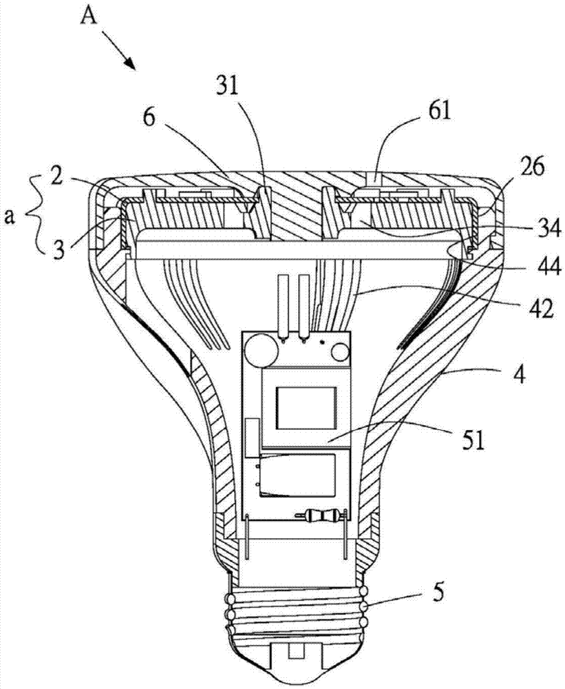
[0136] The present invention relates to an LED lighting device and a manufacturing method thereof, together with seven embodiments and seven sets of system drawings, to illustrate the core technology used in the present invention. In other words, where Figure 1 ~ Figure 1i , is the lighting device of the flat bulb lamp and the manufacturing method thereof according to the first embodiment of the present invention; Figure 2 ~ Figure 2h , about the lighting device of the curved bulb lamp according to the second embodiment of the present invention, and so on. In particular, the main components of the structure of each embodiment of the present invention, and components with the same function are summed up with one component symbol to simplify the description of the present invention.

[0137] see Figure 1e , the lighting device of each embodiment of the present invention is mainly composed of a conductive plate 2 combined with a support frame 3; wherein the conductive plate ...


PUM


Abstract

The invention provides an LED illuminating device and a manufacturing method thereof. The LED illuminating device is mainly characterized in that a metal sheet is stamped and formed into a current-conducting plate with a 3D space, the current-conducting plate is provided with an illuminating circuit, then the current-conducting plate is supported through a supporting frame, and the illuminating device of multiple types is formed. The supporting frame is used for supporting and fixing the current-conducting plate, and the solid curve surface of the formed space of the current-conducting plate is facilitated. The LED illuminating device is further provided with an LED chip welding point protection mechanism used for protecting all LED chip welding points. The LED illuminating device can be suitable for mass production, the manufacturing yield of the device can be increased, and the demands of high radiating efficiency, large illuminating area, material saving, light weight or/and environment protection can be met.

Description

technical field [0001] The present invention relates to a light-emitting diode lighting device, in particular to an LED lighting device and a manufacturing method thereof mainly using a stamping forming technology to form a lighting circuit structure. Background technique [0002] LED lighting devices often use packaged LED chips as light-emitting components. Common packaging forms include: DIP packaged LEDs, SMD packaged LEDs, COB packaged LEDs, CSP packaged LEDs, etc. The above various forms of packaged LEDs are hereinafter referred to as LED chips. ;In addition to the conductive electrode contacts, the LED chip sometimes also has a heat transfer point to accelerate heat conduction to the outside. In many cases, multiple LED bare crystals are packaged on a large aluminum substrate in order to increase the lighting power. Most are much larger than the size of the LED die, also known as large aluminum substrate package. [0003] The common functional requirements and known ...

Claims


Application Information

Patent Timeline
Patent Type & Authority Applications(China)
IPC IPC(8): F21K9/20F21K9/232F21K9/27F21K9/90F21V19/00F21V23/00F21Y115/10
CPCF21K9/90F21V19/002F21V19/0025F21V23/00
Inventor 简焕然蔡茗洋
Owner LONGWIDE TECH
Why Eureka
Try Eureka