Photomask and glass substrate manufacturing method

A manufacturing method and technology for glass substrates, which are applied in the photoengraving process of the pattern surface, the originals for optical mechanical processing, optics, etc., can solve the problems of film breakage, affecting the yield of finished products, short circuit of the common electrode of pixels, etc. The effect of being less prone to breakage and reducing the risk of residues

Inactive Publication Date: 2017-07-07
SHENZHEN CHINA STAR OPTOELECTRONICS TECH CO LTD
View PDF7 Cites 17 Cited by
  • Summary
  • Abstract
  • Description
  • Claims
  • Application Information

AI Technical Summary

Problems solved by technology

This residue will cause a short circuit of the common electrode inside the pixel, resulting in bright spot defects on the panel, which will greatly affect the yield of the finished product, and the excessive taper angle will easily cause the film to break when climbing.
[0005] The conventional photomask structure in the prior art includes a light-transmitting area and a non-light-transmitting area, and some photomask structures also include a part of the light-transmitting area, but the light-transmitting gap between the light-shielding films in the part of the light-transmitting area remains consistent. The transmittance of the mask structure at the taper angle position of the base is still single, but a transitional step is added, and the improvement effect on the taper angle is not ideal

Method used


Image

  • Photomask and glass substrate manufacturing method
  • Photomask and glass substrate manufacturing method
  • Photomask and glass substrate manufacturing method

Examples


Embodiment Construction

[0038] The present invention will be further described below in conjunction with accompanying drawing.

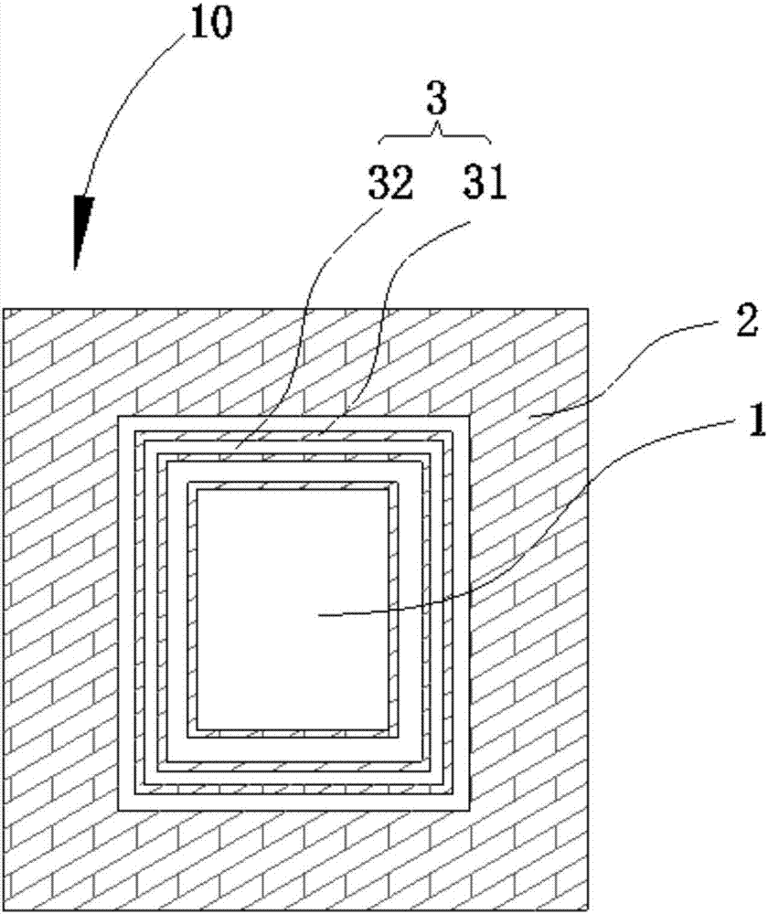
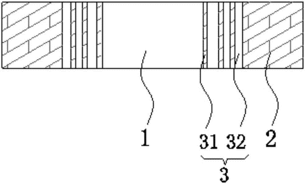
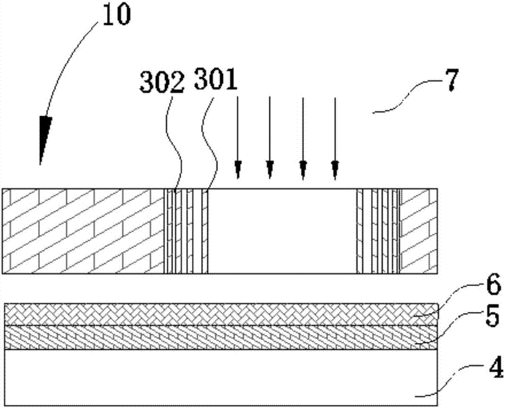
[0039] figure 1 and figure 2 They are respectively a plan view and a cross-sectional view of the photomask of the embodiment of the present invention. see figure 1 and figure 2 , the photomask 10 includes a light-transmitting region 1 and a light-blocking region 2, and the photomask 10 also includes a partially light-transmitting region 3; the partially light-transmitting region 3 is located between the light-blocking region 2 and the light-blocking region 1 to allow light to partially pass through; the partially transparent area 3 includes several identical light-shielding films 31, and light-transmitting gaps 32 are formed between adjacent light-shielding films 31, and the transmittance of the partially light-transmitting area 3 is along the The light-transmitting area 1 gradually decreases toward the light-blocking area 2 .

[0040] It should be noted that the c...


PUM


Abstract

The invention brings forward a photomask, which comprises a photic zone and an antihalation zone. The photomask also comprises a partial photic zone, which is positioned between the antihalation zone and the photic zone to allow light to partially permeate. The partial photic zone comprises several equal shading films. A light-permeable gap is formed between adjacent shading films. Transmittance of the partial photic zone is gradually reduced along the direction from the photic zone towards the antihalation zone. The invention has the following beneficial effects: with the arrangement of the partial photic zone with light-permeable gap width changing on the basis of functional rules along the direction from the photic zone towards the antihalation zone, photoresistive exposure degree of the corresponding partial photic zone is controlled such that the edge of the film after etching and stripping becomes a smooth, cambered surface or other forms of transition surface, it is ensured that a next film folded thereon is not easy to break during climbing, and the residual risk of the film at the taper angle during the follow-up processing treatment is reduced.

Description

technical field [0001] The invention relates to the technical field of liquid crystal display production, in particular to a method for manufacturing a photomask and a glass substrate. Background technique [0002] With the development of display technology, liquid crystal displays (Liquid Crystal Display, LCD) and other flat-panel display devices are widely used in various consumer electronic products such as TVs and computers due to their advantages of high image quality, power saving, and thin body. Main stream in the display device. [0003] Usually, the liquid crystal display panel consists of a color filter substrate (Color Filter, CF), a thin film transistor substrate (Thin Film Transisitor, TFT), and a liquid crystal (Liquid Crystal, LC) and a sealant frame sandwiched between the color filter substrate and the thin film transistor substrate. . Its molding process generally includes: front-end array (Array) process (thin film, yellow light, etching and stripping), m...

Claims


Application Information

Patent Timeline
Patent Type & Authority Applications(China)
IPC IPC(8): G03F1/38G02F1/13
CPCG02F1/1303G03F1/38
Inventor 柳铭岗
Owner SHENZHEN CHINA STAR OPTOELECTRONICS TECH CO LTD
Why Eureka
Try Eureka