
OLED display panel, manufacture method therefor and display device

A display panel and display device technology, applied in semiconductor/solid-state device manufacturing, organic semiconductor devices, semiconductor devices, etc., can solve the problems of low light output rate of OLED display panels, improve brightness and light output rate, simplify process, improve The effect of production efficiency

Active Publication Date: 2017-07-11
BOE TECH GRP CO LTD
View PDF3 Cites 49 Cited by
  • Summary
  • Abstract
  • Description
  • Claims
  • Application Information

AI Technical Summary

Problems solved by technology

[0005] In order to solve the problem of low light extraction rate of existing OLED display panels, embodiments of the present invention provide an OLED display panel, a manufacturing method thereof, and a display device

Method used


Image

  • OLED display panel, manufacture method therefor and display device
  • OLED display panel, manufacture method therefor and display device
  • OLED display panel, manufacture method therefor and display device

Examples


Embodiment Construction

[0041] In order to make the object, technical solution and advantages of the present invention clearer, the implementation manner of the present invention will be further described in detail below in conjunction with the accompanying drawings.

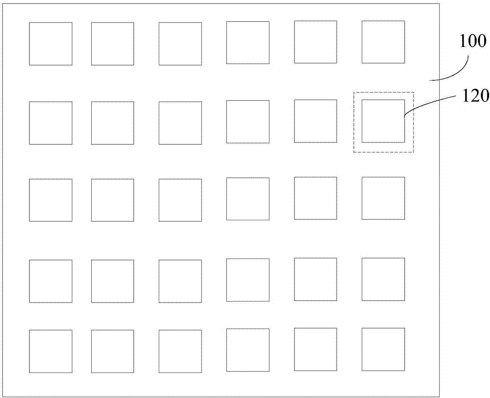
[0042] figure 1 is a schematic structural diagram of an OLED display panel provided by an embodiment of the present invention, as shown in figure 1 As shown, the OLED display panel includes a base substrate 100 and a plurality of OLEDs 120 disposed on the base substrate 100, and the plurality of OLEDs 120 are arranged in an array.

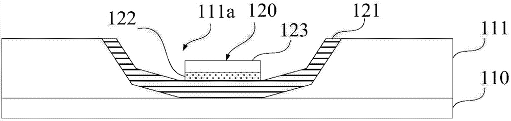
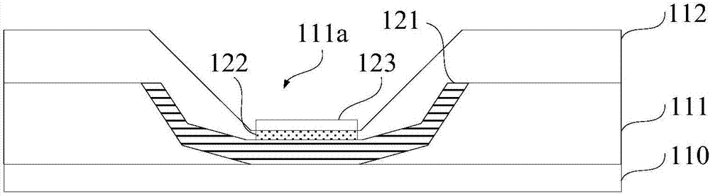
[0043] figure 2 yes figure 1 Schematic cross-section at the dotted box in . Such as figure 2 As shown, the base substrate 100 is further provided with a first pixel definition layer 111 , the first pixel definition layer 111 has a plurality of openings 111 a arranged in an array, and each opening 111 a is correspondingly provided with an OLED 120 . Each OLED 120 includes a first electrode 121, a ligh...


PUM


Abstract

The invention discloses an OLED display panel, a manufacture method therefor and a display device and belongs to the field of display devices. The OLED display panel comprises a substrate base plate, a first pixel definition layer arranged on the substrate base plate and a plurality of OLEDs, wherein a plurality of openings arranged in an array manner are placed on the first pixel definition layer, and each opening is correspondingly provided with an OLED; each OLED comprises a first electrode, an illuminating layer and a second electrode; each first electrode is arranged on a bottom part and a side wall of a corresponding opening, the illuminating layer and the second electrode are orderly arranged on the first electrode, the first electrode is used for reflecting light emitted by the OLED, the side wall of the opening is covered with the first electrode of the OLED, and therefore a reflecting face is formed; light emitted by the OLED can be reflected toward a side, far away from the substrate base plate, of the OLED; light rays can be prevented from entering the first pixel definition layer, and therefore luminance and a light traction rate of the display panel can be improved.

Description

technical field [0001] The invention relates to the field of display devices, in particular to an OLED display panel, a preparation method thereof, and a display device. Background technique [0002] Currently common display devices include passive light emitting display devices (such as liquid crystal display devices) and active light emitting display devices (such as OLED (Organic Light Emitting Diode, organic light emitting diode) display devices). Compared with the passive light-emitting display device, it has the advantages of smaller thickness, low power consumption, fast response speed, etc., so the active light-emitting display device has greater market competitiveness. [0003] The OLED display device includes an OLED display panel. The OLED display panel includes a plurality of OLEDs. Each OLED usually includes an anode, an organic light-emitting layer and a cathode. In an OLED display panel, the anode is usually first fabricated on the substrate, and then the An ...

Claims


Application Information

Patent Timeline
Patent Type & Authority Applications(China)
IPC IPC(8): H01L27/32H01L51/52H01L51/56
CPCH10K59/122H10K59/80518H10K59/80515H10K59/80521H10K59/878H10K2102/351H10K50/856H10K50/813H10K50/818H10K50/822H10K50/828H10K71/00
Inventor 张微
Owner BOE TECH GRP CO LTD
Features
  • Generate Ideas
  • Intellectual Property
  • Life Sciences
  • Materials
  • Tech Scout
  • Unparalleled Data Quality
  • Higher Quality Content
  • 60% Fewer Hallucinations
Learn More