A novel method of transferring graphene film and the preparation method of sensor

A graphene film and graphene composite technology, applied in the field of graphene, can solve the problems of PMMA film wrinkles, graphene damage, and resin layer cannot be removed, and achieve the effect of reducing operation difficulty, reducing cost and low price

Inactive Publication Date: 2019-11-08
成都川烯科技有限公司
View PDF3 Cites 0 Cited by
  • Summary
  • Abstract
  • Description
  • Claims
  • Application Information

AI Technical Summary

Problems solved by technology

[0003] At present, the transfer of graphene film is mainly through PMMA method, resin transfer method or thermal release tape method, but there are certain operational difficulties or inherent defects.
When the PMMA method transfers graphene, because PMMA is difficult to dissolve, it can only reduce the thickness of PMMA, so it is very easy to destroy the PMMA film during operation, thereby destroying the graphene, and when PMMA transfers graphene, the action of picking up the PMMA film is very easy to cause PMMA. Film wrinkles, affecting the transfer effect of graphene films
The inherent defect of the resin transfer method is that the resin layer as the transfer material cannot be removed, which is an insurmountable shortcoming for the characterization and application of graphene

Method used


Image

  • A novel method of transferring graphene film and the preparation method of sensor

Examples


preparation example Construction

[0029] A method for preparing a sensor, comprising: making a channel electrode on the surface of the graphene film prepared by the above method, making the graphene film into a pattern of a touch sensor, attaching optical glue to the surface of the patterned graphene film and then packaging it. Degassing treatment.

[0030]Graphene film is made by using the above-mentioned method of transferring graphene film. Graphene is a super-strong aluminum compound with a honeycomb structure, flexible and more conductive than silicon. The graphene film obtained by the above method is complete, basically It is non-destructive and has a large area, so the use of the graphene film in the production of sensors can enable the sensor to generate stronger electrical signals.

Embodiment 1

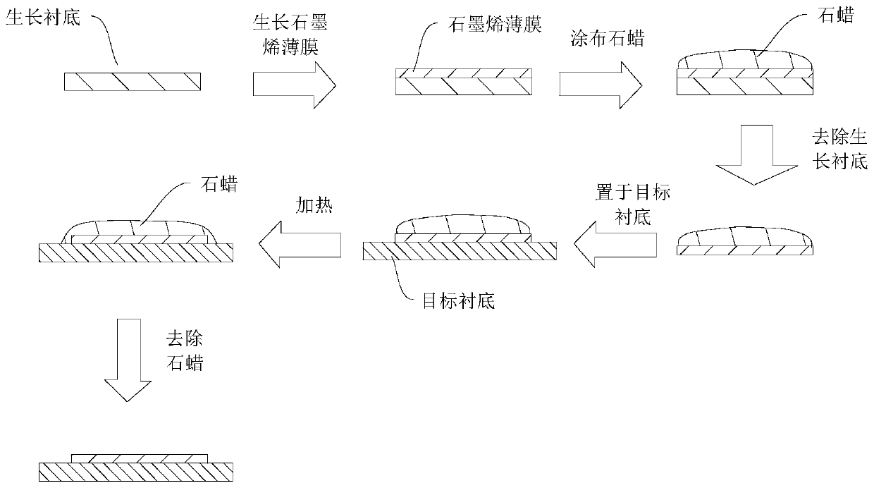
[0033] A novel method for transferring a graphene film, comprising: growing a graphene film by CVD on the surface of a copper foil with a thickness of 30 μm. After the growth is completed, melted paraffin is coated on the surface of the graphene film, and the copper foil substrate is further heated to make the paraffin evenly distributed on the surface of the copper foil, wherein the thickness of the paraffin is about 2mm. After the paraffin is solidified, the copper foil substrate is etched away by chemical etching, and then the graphene surface of the paraffin / graphene composite film is placed on the surface of the silicon wafer. The silicon wafer was heated for 1 min at a temperature of 70° C. to adhere the paraffin wax to the surface of the silicon wafer. Then dissolve the paraffin with xylene, and clean the silicon wafer to completely remove the paraffin, and the transfer of the graphene film is basically completed without damage.

Embodiment 2

[0035] A novel method for transferring a graphene film, comprising: growing a graphene film on the surface of a nickel foil with a thickness of 50 μm by CVD. After the growth is completed, melted paraffin is coated on the surface of the graphene film, and the nickel foil substrate is further heated to make the paraffin evenly distributed on the surface of the nickel foil, wherein the thickness of the paraffin is about 1 mm. After the paraffin is solidified, the nickel foil substrate is etched away by electrochemical corrosion, and then the graphene surface of the paraffin / graphene composite film is placed on the surface of the silicon wafer. The silicon wafer was heated for 1 min at a temperature of 70° C., so that the paraffin wax was completely adhered to the surface of the silicon wafer. Then the paraffin was dissolved with xylene, and the silicon wafer was cleaned to completely remove the paraffin, so that the transfer of the graphene film was basically completed without d...


PUM

PropertyMeasurementUnit
thicknessaaaaaaaaaa
thicknessaaaaaaaaaa
thicknessaaaaaaaaaa

Abstract

The invention provides a novel graphene thin film transferring method and a preparation method of a sensor and relates to the technical field of graphene. The novel graphene thin film transferring method comprises the following steps: covering melted paraffin wax on the surface of a graphene thin film which is formed on the surface of a growth substrate; after the paraffin wax is cured, removing the growth substrate to obtain a paraffin wax / graphene composite thin film; putting the paraffin wax / graphene composite thin film on the surface of a target substrate; heating the target substrate until the paraffin wax is fitted to the target substrate and removing the paraffin wax by utilizing a solvent. The method provided by the invention takes the paraffin wax as a novel transferring medium and is convenient to operate; and the graphene thin film can be basically transferred in a lossless manner. The preparation method of the sensor comprises the following steps: a channel electrode is manufactured on the surface of the graphene thin film prepared using the transferring method and a pattern of a touch sensor is formed by the graphene thin film; and an optical adhesive is fitted on the surface of the graphene thin film and then de-foaming treatment is carried out. By adopting the method provided by the invention, the obtained graphene thin film is complete, basically has no loss and has large area, and can be used for manufacturing the sensor.

Description

technical field [0001] The invention relates to the technical field of graphene, and in particular to a method for transferring a novel graphene film and a method for preparing a sensor. Background technique [0002] Graphene is a single atomic layer two-dimensional crystal with carbon atoms tightly packed in a hexagonal structure. Graphene has excellent properties such as extremely high carrier mobility, high light transmittance, and high strength. It has a huge potential in electronic devices. Value. In order to fabricate graphene electronic devices, large-scale graphene films with excellent electrical properties must first be fabricated and transferred to a suitable target substrate. The transfer technology of graphene film is the key factor restricting the development of graphene film. [0003] At present, the transfer of graphene film is mainly through PMMA method, resin transfer method or thermal release tape method, but there are certain operational difficulties or ...

Claims


Application Information

Patent Timeline
Patent Type & Authority Patents(China)
IPC IPC(8): C01B32/194G01D5/14
CPCG01D5/14
Inventor 周培邓广才朱小英
Owner 成都川烯科技有限公司
Why Eureka
Try Eureka