Surface enhanced Raman scattering substrate and preparation method thereof

A surface-enhanced Raman and substrate technology, applied in Raman scattering, sputtering plating, ion implantation plating, etc., can solve the problems of low Raman signal amplification, high price of Raman chips, and low sensitivity, and achieve Effects of Sensitivity Improvement and Raman Enhancement Performance

Pending Publication Date: 2017-07-14
SOUTH UNIVERSITY OF SCIENCE AND TECHNOLOGY OF CHINA
View PDF5 Cites 2 Cited by
  • Summary
  • Abstract
  • Description
  • Claims
  • Application Information

AI Technical Summary

Problems solved by technology

[0008] In view of the relatively low sensitivity of the SERS substrate in the prior art and the small Raman signal enhancement factor, the object of the present invention is to provide a surface-enhanced Raman scattering SERS substrate and a preparation method thereof. The SERS substrate of the present invention With high sensitivity, it can greatly enhance the Raman signal, and the maximum Raman signal enhancement factor is 10 10 ~10 13 , which can be used to detect molecular signals of analytes at very low concentrations
Moreover, the preparation process of the present invention is simple, easy to produce on an industrial scale, and low in cost, and can be used to prepare chips, which solves the problems of high relative price of Raman chips and low Raman signal amplification in the market

Method used


Image

  • Surface enhanced Raman scattering substrate and preparation method thereof
  • Surface enhanced Raman scattering substrate and preparation method thereof
  • Surface enhanced Raman scattering substrate and preparation method thereof

Examples


Embodiment 1

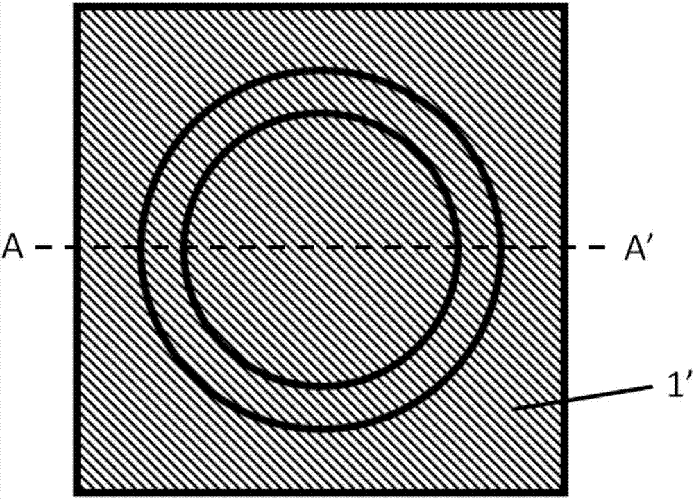
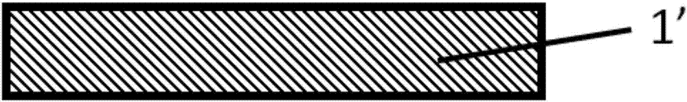
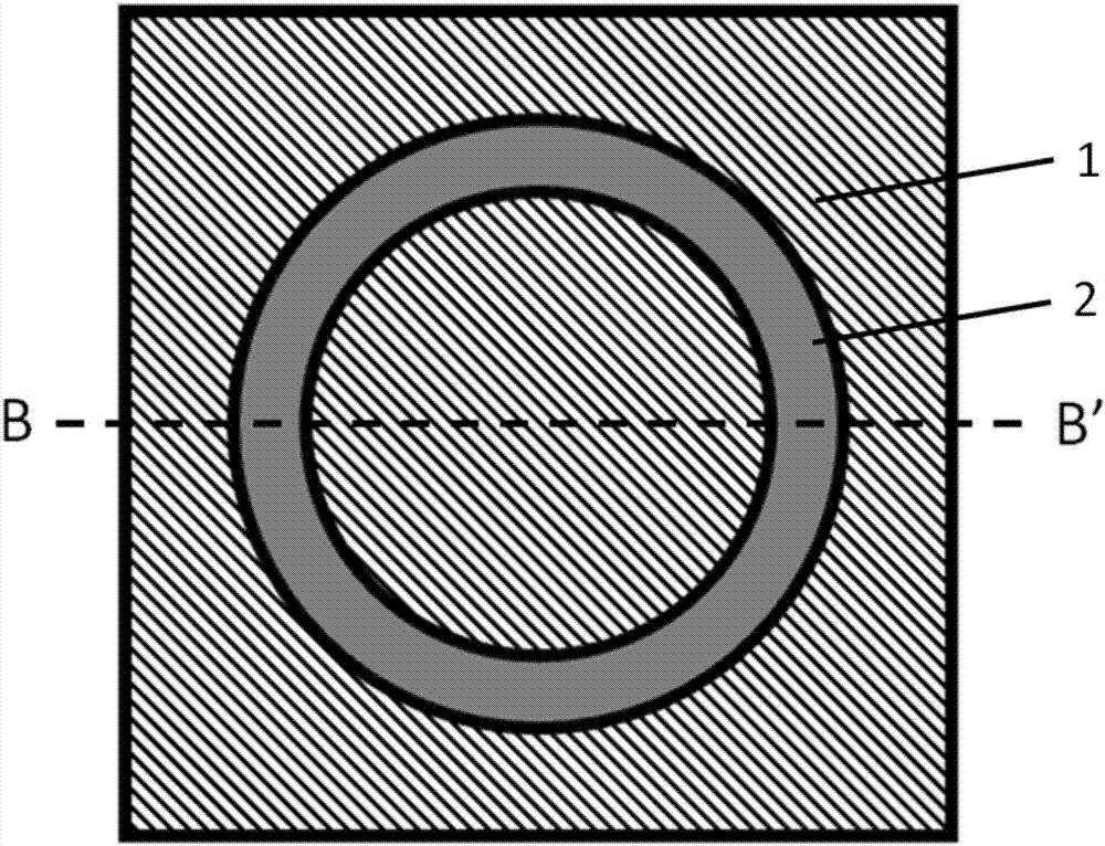
[0091] This embodiment provides a surface-enhanced Raman scattering SERS substrate, the SERS substrate consists of a 0.12 μm thick first SiO from bottom to top 2 Layer 1, 0.1 μm thick Ag layer with interstitial rings 3, 0.04 μm thick second SiO 2 Layer 4 and two identical 0.04 μm thick equilateral triangular silver flakes 5 (side length is 127nm);

[0092] Among them, the first SiO 2 Layer 1, Ag layer 3 with interstitial ring and second SiO 2 Layer 4 is a square of the same size, and the side length of the square is 1 μm.

[0093] In the Ag layer 3 with the void ring, the ring inner diameter of the void ring is 0.37 μm, and the outer diameter is 0.47 μm, then the width of the void ring is 100 nm; centers coincide.

[0094] 2 identical equilateral triangles are arranged with vertices facing each other, and these two opposite vertices are located on one central axis of the square, and are located on both sides of the other central axis of the square and are symmetrical; The...

Embodiment 2

[0105] This embodiment provides a SERS substrate, which is the same as the SERS in Embodiment 1 except that the bases of two identical equilateral triangles are 140 nm.

[0106] The preparation method of the SERS substrate of this embodiment, except that the base of the equilateral triangle in the step (6) is 140 nm, other preparation methods and conditions are the same as in the embodiment 1.

[0107] Test results: the maximum Raman signal enhancement factor of the SERS substrate of this embodiment is 4.47*10 12 .

Embodiment 3

[0109] This embodiment provides a SERS substrate, except that the inner diameter of the void ring is 0.45 μm and the outer diameter is 0.55 μm, the other contents are the same as those of the SERS in Embodiment 1.

[0110] The preparation method of the SERS substrate of this embodiment, except that the inner diameter of the ring region in step (1) is 0.45 μm and the outer diameter is 0.55 μm, other preparation methods and conditions are the same as in Example 1.

[0111] Test results: the maximum Raman signal enhancement factor of the SERS substrate of this embodiment is 8.89*10 12 .


PUM


Abstract

The invention discloses a surface enhanced Raman scattering (SERS) substrate and a preparation method thereof. The SERS substrate is composed of a first SiO2 layer, an Ag layer with a gap circular ring, a second SiO2 layer and two equilateral-triangle-shaped silver sheets from bottom to top, wherein the second SiO2 layer is composed of two parts: one part is located on the surface of the Ag layer with the gap circular ring and the other part is located on a connecting surface of the gap circular ring and the first SiO2 layer; the two equilateral-triangle-shaped silver sheets are located on the second SiO2 layer located in an inner diameter region of the gap circular ring; the minimum distance between the apex of one equilateral-triangle-shaped silver sheet and the apex of the other equilateral-triangle-shaped silver sheet is 1nm to 15nm. According to the SERS substrate provided by the invention, the maximum Raman signal enhancement time can reach 10<13> and the average Raman signal enhancement time can reach 10<6>; the SERS substrate has a relatively good Raman enhancing effect.

Description

technical field [0001] The invention belongs to the technical field of micro-nano structure devices, and relates to a surface-enhanced Raman scattering (surface-enhanced Raman scattering, SERS) substrate and a preparation method thereof. Background technique [0002] When light is scattered by atoms or molecules, most of the photons are elastically scattered, that is, the frequency of the scattered light is the same as that of the incident light, which is called Rayleigh scattering; The frequency is different from the incident light, also known as Raman scattering. [0003] Raman scattering can accurately reflect the information of the vibration energy level of molecules, so it is regarded as the "fingerprint" of molecules and is widely used in the detection of substances. At the same time, Raman scattering spectroscopy detection is a method of material structure analysis that does not require labeling of the sample to be detected, and has the characteristics of non-destruc...

Claims


Application Information

Patent Timeline
IPC IPC(8): G01N21/65C23C14/04C23C14/10C23C14/18
CPCG01N21/658C23C14/04C23C14/10C23C14/18
Inventor 程鑫陈巍元姜有为李维昊
Owner SOUTH UNIVERSITY OF SCIENCE AND TECHNOLOGY OF CHINA
Why Eureka
Try Eureka