Formation method for assistance graph

A technology of auxiliary graphics and graphics, which is applied to the photoplate-making process of the patterned surface, the original for photomechanical processing, optics, etc., can solve the problems of large verification time and small process window, and achieve the goal of saving chip verification time Effect

Inactive Publication Date: 2017-07-14
SEMICON MFG INT (SHANGHAI) CORP +1
View PDF5 Cites 15 Cited by
  • Summary
  • Abstract
  • Description
  • Claims
  • Application Information

AI Technical Summary

Problems solved by technology

[0005] The existing methods for forming sub-resolution auxiliary patterns have a small process window, are easy to form patterns on photoresist, and require a lot of verification time

Method used


Image

  • Formation method for assistance graph
  • Formation method for assistance graph
  • Formation method for assistance graph

Examples


Embodiment Construction

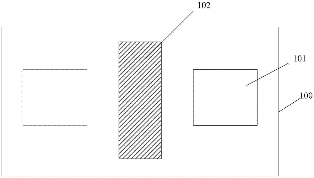
[0029] As mentioned in the background technology, after the auxiliary pattern is formed in the prior art, chip verification is required to determine whether the added auxiliary pattern can form a pattern on the photoresist; until the sub-resolution auxiliary pattern cannot be formed on the photoresist Form a pattern; if the sub-resolution auxiliary pattern can form a pattern on the photoresist, it is necessary to adjust the sub-resolution auxiliary pattern, and then perform chip verification until the sub-resolution auxiliary pattern cannot be formed on the photoresist. Forming a pattern on the glue requires a lot of chip verification time.

[0030] In an embodiment of the present invention, through optical simulation, the simulated light intensity value when passing through the initial auxiliary pattern and reaching the photoresist during the photolithography process is obtained. If the maximum value of the simulated light intensity value is less than the exposure critical val...


PUM


Abstract

Disclosed is a formation method for an assistance graph. The formation method comprises the steps of providing a to-be-etched graph which comprises a plurality of main graphs; setting an initial assistance graph in the to-be-etched graph according to the distribution density of the main graphs in the to-be-etched graph; establishing an optical model according to parameter information of a to-be-implemented photoetching process; performing optical simulation through the optical model to obtain a simulation light intensity value when light penetrates through the initial assistance graph to arrival at photoresist in the photoetching process; if the maximum of the simulation light intensity value is less than an exposure critical value, completing the setting of the assistance graph; and if the maximum of the simulation light intensity value is greater than or equal to the exposure critical value, reducing the width of the initial assistance graph until the obtained simulation light intensity value is less than the exposure critical value, and completing the setting of the assistance graph. By virtue of the formation method, chip verification on the set assistance graph is not needed, so that chip verification time can be saved, and it is ensured that the assistance graph does not appear on the photoresist in the actual photoetching process.

Description

technical field [0001] The invention relates to the technical field of semiconductors, in particular to a method for forming an auxiliary pattern. Background technique [0002] With the development of integrated circuit production technology, the feature size of semiconductor devices is continuously reduced, and the design scale is also continuously expanded, which makes the design of semiconductor devices more and more complex. When the feature size is close to the theoretical resolution limit of the lithography system, the image formed on the wafer after lithography will produce obvious distortion, which will lead to a serious decline in the quality of lithography. In order to solve this problem, the industry proposes and adopts resolution enhancement technology, which mainly includes correction methods such as off-axis illumination, optical proximity correction, phase shift mask, and sub-resolution auxiliary pattern (SRAF). [0003] Among them, the sub-resolution auxilia...

Claims


Application Information

Patent Timeline
Patent Type & Authority Applications(China)
IPC IPC(8): G03F1/36
CPCG03F1/36
Inventor 杨青
Owner SEMICON MFG INT (SHANGHAI) CORP
Why Eureka
Try Eureka