
Chip resistor element and method for forming same

A technology for resistors and resistor layers, applied in the direction of resistor parts, resistors, electrical components, etc., can solve problems such as lowering of plating characteristics, delamination, and inability to form properly

Active Publication Date: 2017-07-18
SAMSUNG ELECTRO MECHANICS CO LTD
View PDF7 Cites 9 Cited by
  • Summary
  • Abstract
  • Description
  • Claims
  • Application Information

AI Technical Summary

Problems solved by technology

However, according to this method, it is difficult to ensure a high level of electrical conductivity, and also the plating characteristics are lowered so that the plating layer for the external electrodes cannot be properly formed or the adhesive strength of the plating layer with respect to the underlying structure is lowered, so that problems such as layered problem

Method used


Image

  • Chip resistor element and method for forming same
  • Chip resistor element and method for forming same
  • Chip resistor element and method for forming same

Examples


example 1

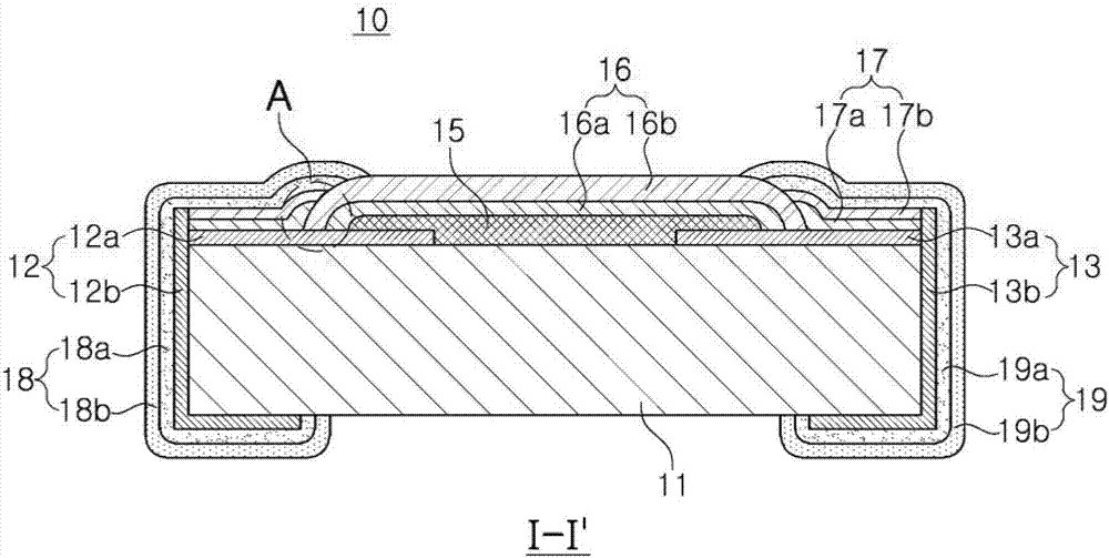
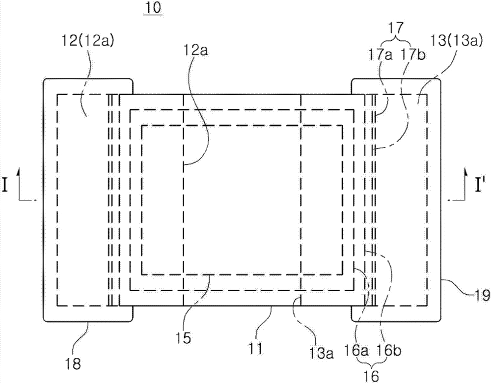
[0066] Based on the conditions of this disclosure, with figure 1 The first electrode protection layer and the second electrode protection layer (for example, 17a and 17b) were fabricated in a chip resistor element similar to the chip resistor element shown in .

[0067] First, upper electrodes (for example, 12a and 13a) are formed using a paste containing Ag as a main component. A paste in which carbon nanotubes and epoxy resin are mixed with each other at a weight ratio of 3:97 is used to form the first electrode protective layer (for example, 17a). A product having a diameter of about 8 nm and a length of 10 μm to 15 μm was used as the carbon nanotube. Use the paste of CuNi alloy (Ni: 70wt%), carbon nanotube and epoxy resin to mix each other according to the ratio of 94:1:5 to form the second electrode protection layer (for example, 17a) on the first electrode protection layer (for example, 17a). , 17b). Then, external electrodes (for example, 18, 19) are formed by succes...

example 2

[0078] Invention example 2: Evaluation of CuNi alloy

[0079] The evaluation of the CuNi alloy effectively employed in this exemplary embodiment was performed. While changing the ratio of Cu to Ni (Ni content: 0wt%, 20wt%, 45wt%, 80wt%, 100wt%), the anti-sulfidation characteristics and specific resistance values ​​of the alloy powder particles of the respective samples were measured. An electrode protective layer (for example, 17 ) was manufactured by mixing 90 wt % of alloy powder particles having a composition based on the conditions described above with 10 wt % of epoxy resin. The electrode protection layer prepared in this experiment may be the second electrode protection layer (for example, 17b).

[0080] First, an alloy ratio-based FoS test was performed on each sample. The FoS test is performed by the same method as described above. In addition, the change in the specific resistance value of each sample based on the amount of carbon nanotubes added was also measure...


PUM


Abstract

Provided are a chip resistor element and a method for forming the same. The chip resistor element includes an insulating substrate, a resistor layer, first and second internal electrodes, a resistor protection layer, first and second electrode protection layers, and first and second external electrodes. The resistor layer is on the insulating substrate, the first and second internal electrodes are on respective sides of the resistor layer, and the resistor protection layer covers the resistor layer and extends onto portions of the internal electrodes. The first electrode protection layers are on the first and second internal electrodes so as to overlap with portions of the resistor protection layer and contain first conductive powder particles and resin, while the second electrode protection layers are disposed on the first electrode protection layers and contain second conductive powder particles and resin. A content of resin in the second electrode protection layer is lower than in the first electrode protection layer.

Description

[0001] This application claims the benefit of priority from Korean Patent Application No. 10-2016-0002698 filed with the Korean Intellectual Property Office on Jan. 8, 2016, the disclosure of which is hereby incorporated by reference in its entirety. technical field [0002] The present disclosure relates to a chip resistor element. Background technique [0003] Generally, when a chip resistor element is used for a long time while being exposed to the external environment, undesired reactions occur in components of the chip resistor element such as internal electrodes, deteriorating the reliability of the chip resistor element. Reduced, or the performance of chip resistor components will be lost. For example, metals such as silver (Ag) that are commonly used as materials for internal electrodes can be easily sulfided, forming undesired reactants (e.g., Ag 2 S), leading to disconnection. [0004] Generally, in order to solve these problems, a method of replacing the interna...

Claims


Application Information

Patent Timeline
Patent Type & Authority Applications(China)
IPC IPC(8): H01C7/00H01C1/034H01C1/142
CPCH01C1/034H01C1/142H01C7/003H01C7/001H01C17/02H05K3/3442H01C1/01H01C1/148H01C17/006H01C17/24H01C17/28H05K1/181H05K2201/10022Y02P70/50H01C7/18
Inventor 尹长锡金亨珉韩镇万
Owner SAMSUNG ELECTRO MECHANICS CO LTD
Learn More