
Light-operated IGBT realization method and structure based on tunneling effect

A technology of tunneling effect and realization method, which is applied in the direction of sustainable manufacturing/processing, electrical components, climate sustainability, etc., can solve the problems of IGBT insulation isolation and long state transition time, and achieve short photoelectric effect response time and formation The effect of short time, shortened state transition time and delay time

Inactive Publication Date: 2017-07-21
INST OF FLUID PHYSICS CHINA ACAD OF ENG PHYSICS
View PDF4 Cites 0 Cited by
  • Summary
  • Abstract
  • Description
  • Claims
  • Application Information

AI Technical Summary

Problems solved by technology

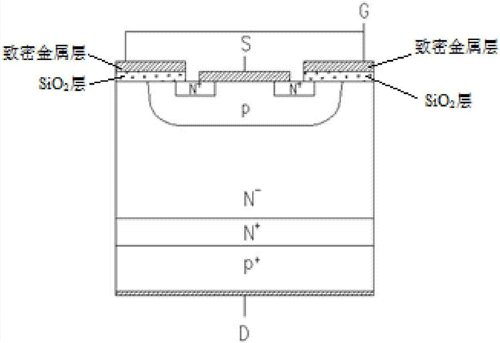
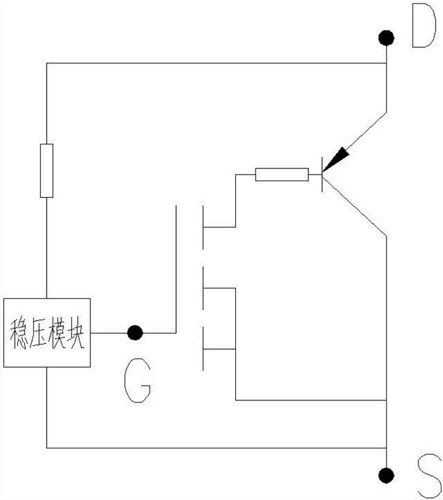
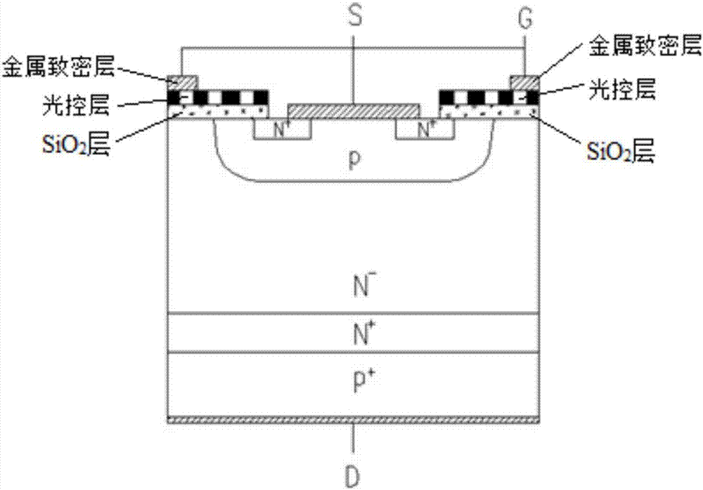
By designing a special gate structure (increasing the photocontrol layer, and reducing the area of ​​the dense metal layer used for the electrode lead-out connection of the gate to the range of the outer ring layer) and making it connect with the IGBT source through the current limiting resistor and the voltage stabilizing module , The IGBT drain is connected, and the laser pulse is used to control the formation of the conductive channel under the gate to control the on-off of the IGBT, which is used to solve the problems of IGBT insulation isolation and long state transition time

Method used


Image

  • Light-operated IGBT realization method and structure based on tunneling effect
  • Light-operated IGBT realization method and structure based on tunneling effect
  • Light-operated IGBT realization method and structure based on tunneling effect

Examples


Embodiment Construction

[0034] All features disclosed in this specification, or steps in all methods or processes disclosed, may be combined in any manner, except for mutually exclusive features and / or steps.

[0035] Any feature disclosed in this specification, unless specifically stated, can be replaced by other alternative features that are equivalent or have similar purposes. That is, unless expressly stated otherwise, each feature is one example only of a series of equivalent or similar features.

[0036] Relevant description of the present invention:

[0037] 1. The low resistivity silicon layer refers to the resistivity lower than 10 4 ohm / cm layered structure of silicon.

[0038] 2. The P region below the gate region refers to figure 2 Below the middle grid, N - District and N + the area between the districts.

[0039] 3. The gate blocking potential is 5-15V lower than the source potential.

[0040] Design process: The typical structure of the IGBT in the prior art is as follows figu...


PUM


Abstract

The invention relates to the semiconductor device design field, provides a light-operated IGBT realization method and device and aims to solve problems in the prior art. Laser pulses are utilized to control formation of a conductive channel in a semiconductor material at a lower portion of a grid, on and off of an IGBT are controlled, and IGBT insulation isolation and long state transition time problems are solved. A light-operated layer for conduction and light transmission is manufactured above a SiO2 layer at a bottom surface of a grid region of the IGBT; a compact metal layer is generated on a top layer of an outer ring layer of the grid, and a leading wire on the metal layer is connected with an outer electrode of the grid of a packaging casing of the IGBT; an inner ring layer is connected with the outer ring layer through the conductive light-operated layer; when the laser pulses irradiate the grid of the IGBT, namely the inner ring layer of the light-operated layer, P-region width below the grid is substantially compressed, under the action of the tunneling effect, N+ and N- region carriers are made to transit through a P region, and thereby IGBT conduction is realized.

Description

technical field [0001] The invention relates to the field of semiconductor device design, in particular to a tunneling effect-based light control IGBT realization method and structure. Background technique [0002] Currently, IGBTs are designed as voltage-controlled devices ( figure 1 ), the gate is a metal electrode, a sufficiently high forward drive voltage signal is applied between the gate and the source, and an inversion layer is formed in the P region under the gate, that is, an N-type conduction channel. Through this channel, electrons from the source region of the N + District flows to N - The drift region, up to the N region adjacent to the drain, puts the IGBT into the conduction state. When the positive drive voltage between the gate and the source disappears, and the gate and the source are at the same potential or lower than the source potential, the IGBT is turned off. Therefore, at present, the conduction of the IGBT is controlled by the gate drive voltage...

Claims


Application Information

Patent Timeline
Patent Type & Authority Applications(China)
IPC IPC(8): H01L31/18H01L31/11H01L31/0224
CPCH01L31/022408H01L31/1105H01L31/1804Y02P70/50
Inventor 赵娟李博婷李洪涛李波黄宇鹏张信
Owner INST OF FLUID PHYSICS CHINA ACAD OF ENG PHYSICS
Learn More