Display panel and display device

A display panel and microcavity technology, applied in the direction of electrical components, electrical solid devices, circuits, etc., can solve the problems of increasing process steps and costs, increasing power consumption of display screens, and improving process difficulty, so as to reduce process steps and costs, Reduced power consumption and high color purity

Active Publication Date: 2017-07-25
SOUTH CHINA UNIV OF TECH
View PDF10 Cites 24 Cited by
  • Summary
  • Abstract
  • Description
  • Claims
  • Application Information

AI Technical Summary

Problems solved by technology

However, considering that after the spectrum of a certain wavelength is enhanced, other spectra weakened by the length of the optical cavity appear nearby. In this way, a color filter layer is required to filter out these miscellaneous peaks during the colorization process. About 50% of the light will be absorbed, resulting in reduced luminous brightness and increased power consumption of the display; on the other hand, if the color filter layer is processed on the OLED, it must be required that the color filter layer be realized at a temperature lower than 90°C. , increasing the difficulty of the process
If the color filter layer is fabricated on an external substrate, precision alignment and display substrate bonding are required later, which increases process steps and costs

Method used


Image

  • Display panel and display device
  • Display panel and display device
  • Display panel and display device

Examples


Embodiment Construction

[0023] The technical solutions of the present invention will be further described below in conjunction with the accompanying drawings and through specific implementation methods. It should be understood that the specific embodiments described here are only used to explain the present invention, but not to limit the present invention. In addition, it should be noted that, for the convenience of description, only some structures related to the present invention are shown in the drawings but not all structures.

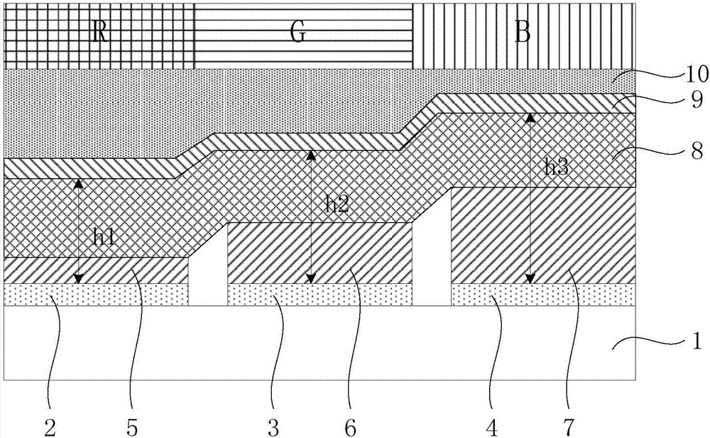
[0024] figure 1 It is a structural schematic diagram of an existing display panel. Such as figure 1 As shown, the existing display panel can include a plurality of pixel areas, each pixel area includes a red sub-pixel area, a green sub-pixel area and a blue sub-pixel area; the display panel also includes a substrate 1; a reflective electrode located on the substrate One side of the bottom 1 includes a red light reflective electrode 2 located in the red sub-pixel area,...


PUM


Abstract

The invention discloses a display panel and a display device. The display panel comprises a reflection electrode layer; a microcavity structure layer formed on the side, away from a substrate, of a first electrode layer and including a first microcavity structure for transmitting red light, a second microcavity structure for transmitting green light, and a third microcavity structure for transmitting blue light; and a semitransparent electrode layer formed on the side, away from the substrate, of the microcavity structure layer. The microcavity structure layer comprises a white light emitting layer including a red light-emitting peak, a green light-emitting peak and a blue light-emitting peak the positions of which satisfy a condition that a difference between the red light-emitting peak and the green light-emitting peak is greater than or equal to the sum of the half-peak width of the red light-emitting peak and the half-peak width of the green light-emitting peak, and a difference between the green light-emitting peak and the blue light-emitting peak is greater than or equal to the sum of the half-peak width of the green light-emitting peak and the half-peak width of the blue light-emitting peak. The process cost and the power consumption of the display device are reduced and the brightness of the display device is increased.

Description

technical field [0001] Embodiments of the present invention belong to the field of display technology, and relate to a display panel and a display device. Background technique [0002] The technologies for realizing the colorization of Organic Light-Emitting Diode (OLED) include two mainstream technologies, that is, micro-cavity effect RGB pixel independent light-emitting technology, and white light-emitting materials combined with color filter layer technology. [0003] Micro-cavity effect RGB pixels need to use precise metal shadow mask and pixel alignment technology to prepare red, green and blue primary color light-emitting centers of micro-cavity effect to achieve colorization. The shadow mask method is difficult to ensure the positioning accuracy of sub-pixels, and it is relatively difficult to realize a display panel with high pixel density. Moreover, the precision metal shadow mask is expensive, which will lead to an increase in cost. [0004] The method of combinin...

Claims


Application Information

Patent Timeline
Patent Type & Authority Applications(China)
IPC IPC(8): H01L27/32H01L51/52H01L51/50
CPCH10K59/35H10K50/115H10K50/852
Inventor 王磊邹建华陶洪徐苗李洪濛彭俊彪
Owner SOUTH CHINA UNIV OF TECH
Why Eureka
Try Eureka