

DC restoration circuit with DC offset compensation function
A DC recovery and DC offset technology, applied in DC-coupled DC amplifiers, amplifiers with semiconductor devices/discharge tubes, amplifiers with only semiconductor devices, etc., can solve the output signal distortion and low common-mode level at the output And other issues
- Summary
- Abstract
- Description
- Claims
- Application Information
AI Technical Summary
Problems solved by technology
Method used
Image

Examples
Embodiment 1
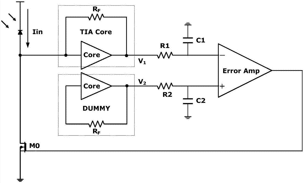
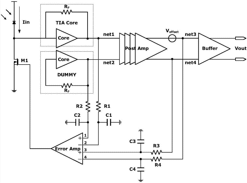
[0027] refer to figure 2 , a DC restoration circuit with a DC offset compensation function, comprising: a transimpedance amplifier TIA, a differential amplifier Post Amp, an error amplifier Error Amp, a dummy amplifier DUMMY, and a switch tube M0;
[0028] The output terminals of the transimpedance amplifier TIA and the virtual amplifier DUMMY are respectively connected to the differential amplifier PostAmp; the error amplifier Error Amp includes two sets of positive and negative input terminals; one set of positive and negative input terminals are respectively connected to the The output terminals of the transimpedance amplifier TIA and the virtual amplifier DUMMY, and another set of positive and negative input terminals are respectively connected to the two output terminals of the differential amplifier Post Amp;
[0029] The output terminal of the error amplifier Error Amp is connected to the gate of the switch tube M1, the source of the switch tube M1 is grounded, and the...
Embodiment 2
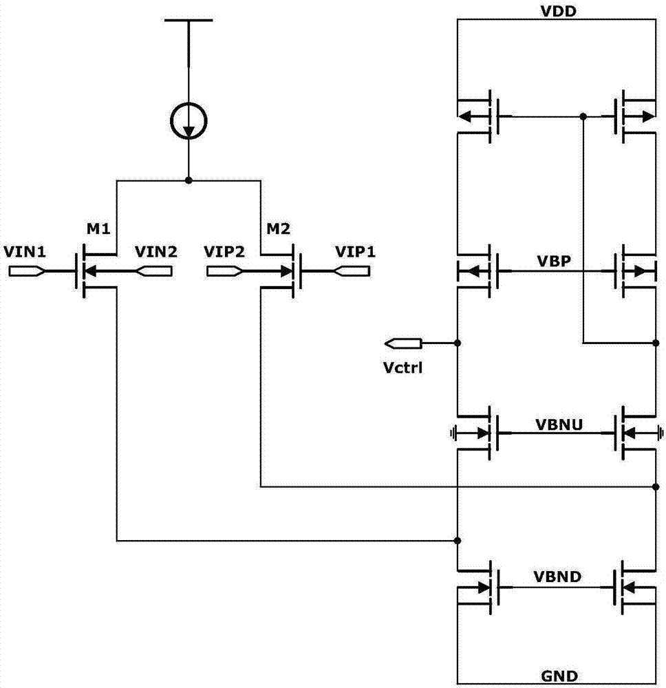
[0042] refer to Figure 4 The difference between this embodiment and Embodiment 1 is that the error amplifier Error Amp adopts the form of voltage addition, and the DC voltages input by two sets of positive and negative input terminals are introduced into the feedback loop of the error amplifier Error Amp. One set of positive and negative input terminals of the error amplifier Error Amp is applied to the gates of the switch tubes M1 and M3, and another set of positive and negative input terminals is applied to the gates of the switch tubes M2 and M47; the switch tubes M1, The sources of M2, M3 and M4 are connected to the feedback loop; and the sources of the switching tubes M1 and M3 are connected, and the sources of the switching tubes M2 and M4 are connected.
[0043] The output voltage of the feedback loop is:
[0044] V ctrl =2·[g m1,2 (V IP1 -V IN1 )+g m3,4 (V IP2 -V IN2 )]·R o
[0045] where g m1,2 for V IP1 and V IN1 The transconductance between, g m3,4 fo...
PUM
 Abstract
Description
Claims
Application Information