

Quantum dot electroluminescent device
A technology of electroluminescent devices and quantum dots, which is applied in the direction of electric solid devices, electrical components, semiconductor devices, etc., can solve the problems of low efficiency of quantum dot electroluminescent devices, and achieve the effect of improving current efficiency
- Summary
- Abstract
- Description
- Claims
- Application Information
AI Technical Summary
Problems solved by technology
Method used
Image

Examples
Embodiment 1
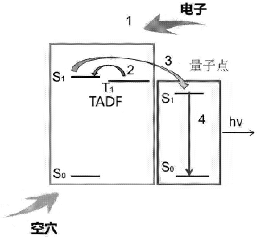
[0091]In this embodiment, the quantum dot material is added to the phosphorescent host material and TADF material (ACRXTN) as the light-emitting layer, and the weight ratio of phosphorescent host material: TADF material: quantum dot material is 60:20:20. ACRXTN is a known TADF material, and the triplet energy level of its CT excited state is higher than that of the n-π excited state, and the difference is between 0 and 0.3 eV.
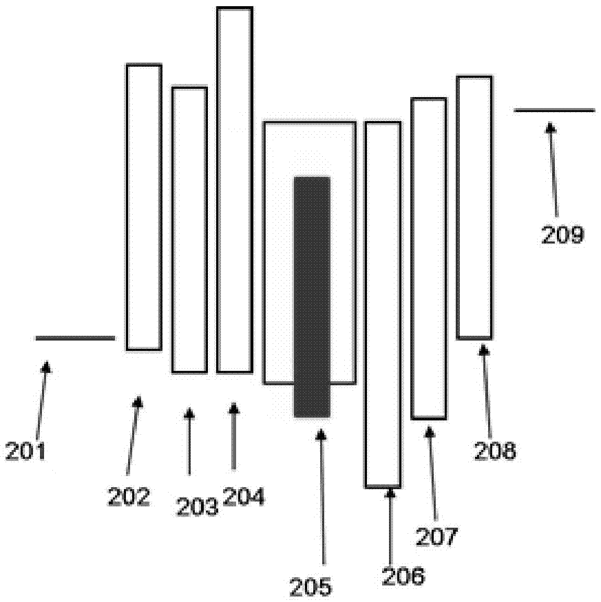
[0092] The quantum dot electroluminescence device structure of the present embodiment is as follows:
[0093] ITO / HATCN(10nm) / NPB(40nm) / TCTA(20nm) / CBP:ACRXTN:CdSe quantum dots(60:20:20)(30nm) / BCP(20nm) / Alq 3 (30nm) / LiF(1nm) / Al(150nm)
[0094]
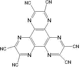
[0095] ACRXTN.
[0096] The experimental data of above-mentioned comparative example and embodiment are shown in the table below:
[0097] Because the colors of the comparative examples and examples are not exactly the same, it is impossible to simply compare the current efficiency. We focus on comparing ...
Embodiment 9 and Embodiment 10
[0108] The structure of the quantum dot electroluminescent device of embodiment 9 and embodiment 10 is similar to embodiment 1, and the quantum dot luminescent layer is made of CBP, TADF material and CdSe quantum dot, and the weight ratio of the three is 60:20:20, the difference The only difference is that different TADF materials are used in each embodiment.
[0109] ITO / HATCN(10nm) / NPB(40nm) / TCTA(20nm) / CBP:TADF material: CdSe quantum dots(60:20:20) (30nm) / BCP(20nm) / Alq 3 (30nm) / LiF(1nm) / Al(150nm)
[0110] The wavelength corresponding to the peak of the luminescence spectrum is 530nm, and the particle size of the CdSe quantum dot is 5.5nm, and the wavelength corresponding to the peak of the absorption spectrum is 514nm.
[0111] The wavelength corresponding to the peak of the emission spectrum of ACRXTN is 490nm.
[0112] The wavelength corresponding to the peak of the emission spectrum of PXZ-TRZ is 550nm.
[0113] The wavelength corresponding to the peak of the emission...
PUM
| Property | Measurement | Unit |
|---|---|---|
| Particle size | aaaaa | aaaaa |
Abstract
Description
Claims
Application Information