Sintered body, sputtering target including the sintered body, and thin film formed using the sputtering target

A technology of sintered body and bulk resistivity, applied in sputtering plating, vacuum evaporation plating, coating, etc., can solve the problems of unsuitable devices, reduced transmittance, and inability to maintain the excellent characteristics of ZnS, so as to improve productivity , low volume resistivity, good water resistance

Active Publication Date: 2020-04-21
JX NIPPON MINING & METALS CORP
View PDF2 Cites 0 Cited by
  • Summary
  • Abstract
  • Description
  • Claims
  • Application Information

AI Technical Summary

Problems solved by technology

[0005] However, adding indium oxide (In 2 o 3 ) in the case of a conductive material, absorption occurs in the short-wavelength region of visible light, and there is a problem that the transmittance decreases
This is not particularly a problem in the use of optical disks (DVDs) using light with a wavelength of 650nm, but when used in display devices such as touch panels and displays, since it is required to be transparent (high transmittance) in the entire visible light region rate), so the problem is not suitable for such devices
In addition, adding alumina (Al 2 o 3 ), there is also a problem that Al is more likely to form a stable sulfide than Zn, so Al combines with sulfur (S) and cannot maintain the excellent characteristics of ZnS

Method used


Image

  • Sintered body, sputtering target including the sintered body, and thin film formed using the sputtering target
  • Sintered body, sputtering target including the sintered body, and thin film formed using the sputtering target
  • Sintered body, sputtering target including the sintered body, and thin film formed using the sputtering target

Examples


Embodiment 1

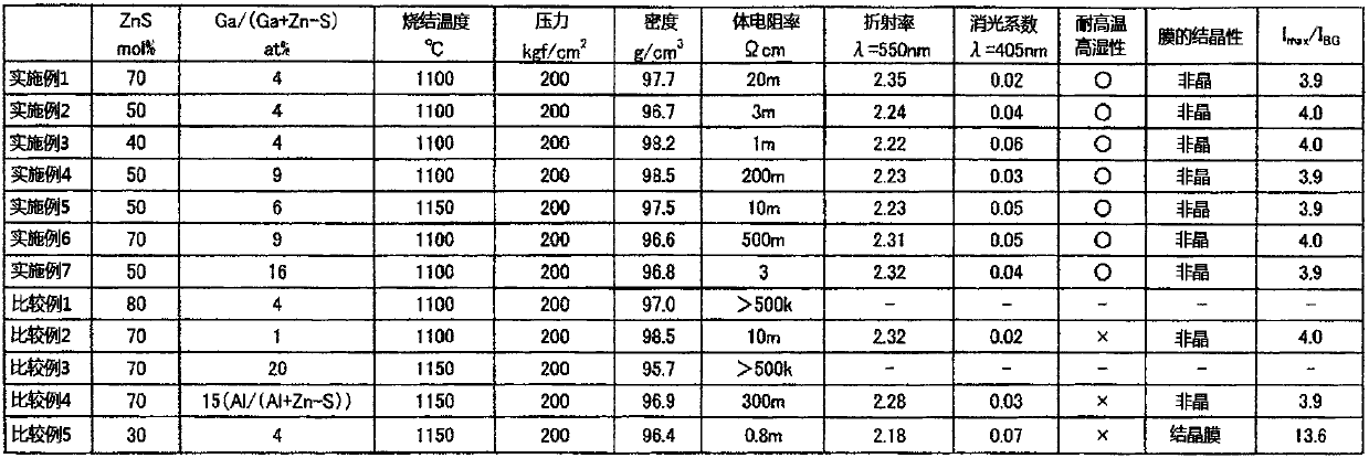
[0091] Deploy Ga 2 o 3 powder, ZnO powder to achieve the atomic ratio shown in Table 1, and mix them. Next, the mixed powder was calcined in the atmosphere at a temperature of 1050° C., and then wet pulverized (using ZrO 2 Microbeads) crushed to an average particle size of 2 μm or less, dried and sieved with a sieve with a mesh size of 150 μm. Then, this finely pulverized powder and ZnS powder were mixed in the compounding ratio described in Table 1, and then, in an Ar atmosphere at a temperature of 1100°C and a pressure of 200kgf / cm 2 hot-pressed sintering conditions.

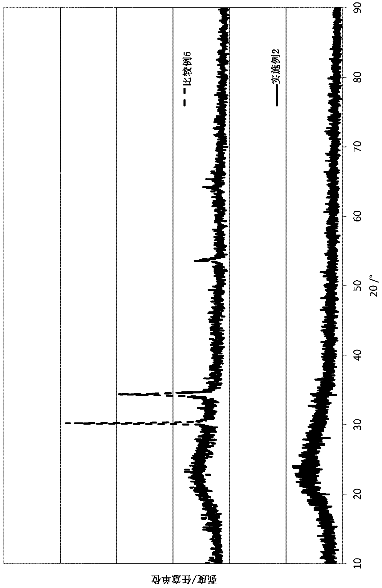
[0092] Then, this sintered body was finished into a sputtering target shape by machining. The volume resistance and relative density of the obtained target were measured. As shown in Table 1, the relative density was 97.7%, the volume resistance was 0.02Ω·cm, and stable DC sputtering was possible. As a result of analyzing the component composition of the target, it was confirmed that the compounding ratio...

Embodiment 2

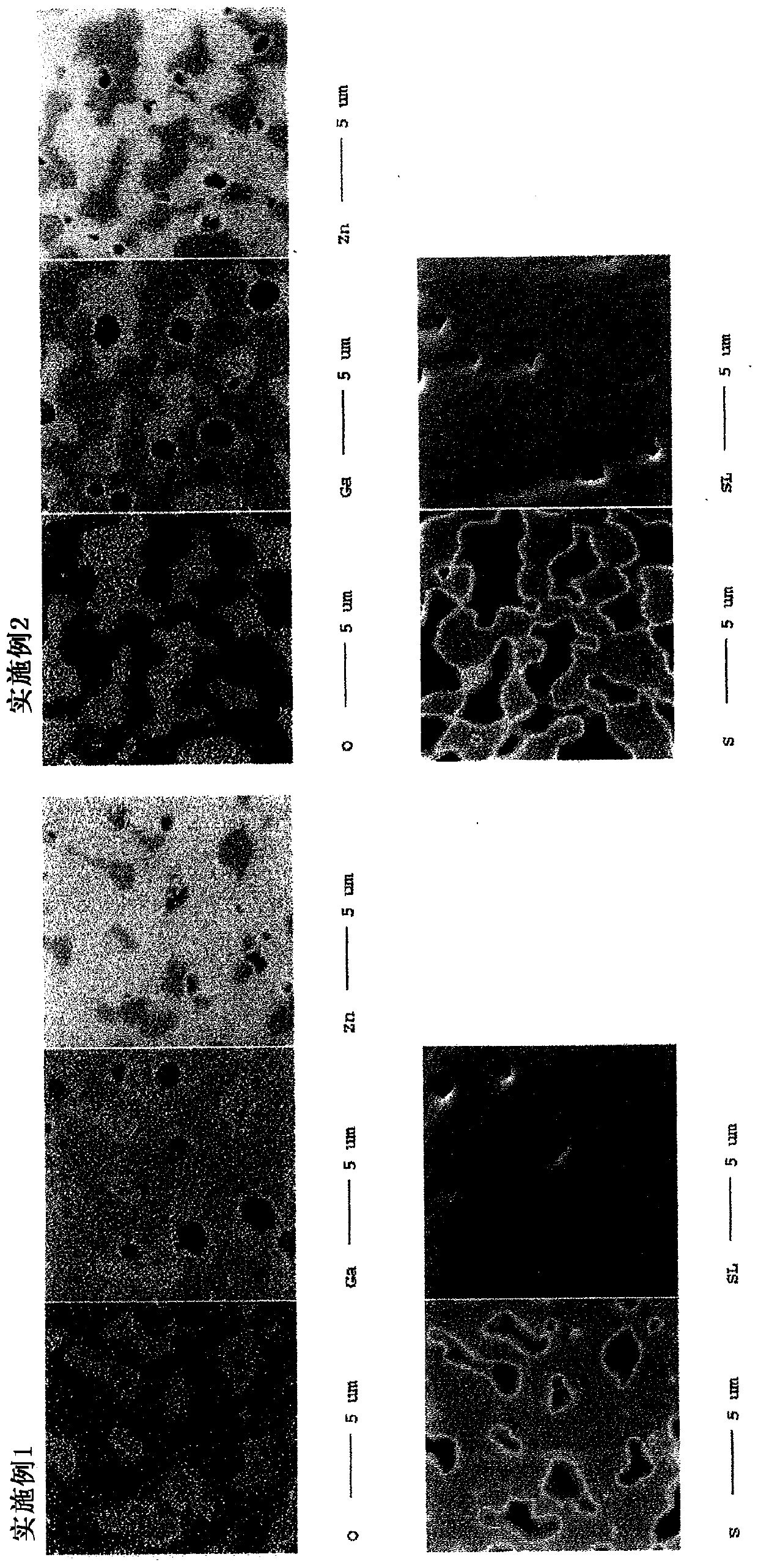
[0097] Deploy Ga 2 o 3 powder, ZnO powder to achieve the atomic ratio shown in Table 1, and mix them. Next, the mixed powder was calcined in the atmosphere at a temperature of 1050° C., and then wet pulverized (using ZrO 2 Microbeads) crushed to an average particle size of 2 μm or less, dried and sieved with a sieve with a mesh size of 150 μm. Then, the finely pulverized powder and the ZnS powder were mixed in the compounding ratio described in Table 1, and hot press sintering was performed in the same manner as in Example 1. Then, this sintered body was finished into a sputtering target shape by machining. The volume resistance and relative density of the obtained target were measured. As shown in Table 1, the relative density was 96.7%, the volume resistance was 0.003Ω·cm, and stable DC sputtering was possible. In addition, the target tissue was observed with EMPA (Electron Probe Microanalyzer), and the results were as follows: figure 1 As shown in , it was confirmed th...

Embodiment 3

[0100] Deploy Ga 2 o 3 powder, ZnO powder to achieve the atomic ratio shown in Table 1, and mix them. Next, the mixed powder was calcined in the atmosphere at a temperature of 1050° C., and then wet pulverized (using ZrO 2 Microbeads) crushed to an average particle size of 2 μm or less, dried and sieved with a sieve with a mesh size of 150 μm. Then, the finely pulverized powder and the ZnS powder were mixed in the compounding ratio described in Table 1, and hot press sintering was performed in the same manner as in Example 1. Then, this sintered body was finished into a sputtering target shape by machining. The volume resistance and relative density of the obtained target were measured. As shown in Table 1, the relative density was 98.2%, the volume resistance was 0.001Ω·cm, and stable DC sputtering was possible. In addition, as a result of observing the target structure with EMPA (electron probe microanalyzer), it was confirmed that oxides containing Ga, Zn, and O were fo...


PUM

PropertyMeasurementUnit
electrical resistivityaaaaaaaaaa
refractive indexaaaaaaaaaa

Abstract

The invention relates to a sintered body, a sputtering target comprising the sintered body and a thin film formed by using the spattering target. The present invention relates to a sintered body or a film containing ZnS and an oxide. The sintered body contains 40 to 70 mol% of ZnS. The oxide in the sintered body contains a composite oxide including at least Zn, Ga, and O. The composition of the sintered body or the film satisfies a relational expression of 4 at% <= Ga / (Ga + Zn - S) <= 18 at%. An objective of the present invention is to provide a sputtering target that is low in bulk resistance value and allows stable DC sputtering. Another objective of the present invention is to provide a thin film as a film for optical adjustment, an optical disc protection film, or a transparent conductive film for various types of display, which has excellent optical or high-temperature high-humidity resistance characteristics.

Description

technical field [0001] The present invention relates to a sintered body, a sputtering target including the sintered body, and a thin film formed using the sputtering target. In particular, it relates to a sputtering target capable of DC sputtering and a thin film having desired characteristics. Background technique [0002] In various optical devices such as organic EL, liquid crystal displays, touch panels, and optical discs, when visible light is used, it is necessary for the material used to be transparent, and in particular, it is desired to have high transmittance over the entire visible light region. . For example, ZnS-SiO 2 It is a high-transmittance and flexible material, so it is used as a protective film for optical discs. However, since this material is insulating, there is a problem that DC sputtering cannot be performed. [0003] Therefore, there is a technology that enables DC sputtering by adding a conductive material to ZnS to lower its resistance. For ex...

Claims


Application Information

Patent Timeline
Patent Type & Authority Patents(China)
IPC IPC(8): C23C14/34C23C14/06C23C14/08
CPCC23C14/0629C23C14/082C23C14/086C23C14/3407C04B35/453C04B35/547C04B35/64C04B2235/3286C04B2235/77C04B2235/9646C23C14/3414
Inventor 奈良淳史
Owner JX NIPPON MINING & METALS CORP
Why Eureka
Try Eureka