Preparation method of long period waveguide grating
A waveguide grating and long-period technology, applied in the field of integrated optics, can solve the problems of large modulation voltage, difficult modulation, and low modulation bandwidth, and achieve the effect of low modulation voltage, easy modulation, and high modulation bandwidth
- Summary
- Abstract
- Description
- Claims
- Application Information
AI Technical Summary
Problems solved by technology
Method used
Image
Examples
Embodiment Construction
[0022] The technical solution of the present invention will be described in detail below in conjunction with the accompanying drawings and specific embodiments.
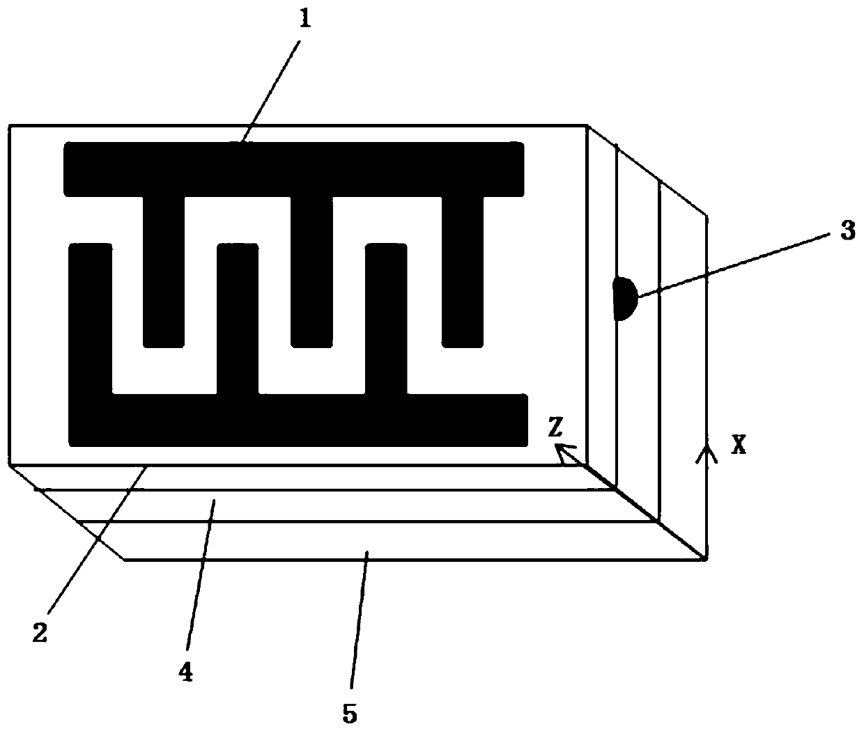
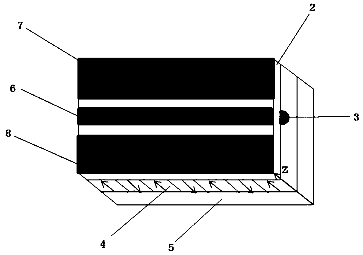
[0023] Such as figure 2 Shown is a schematic structural diagram of a long-period waveguide grating proposed by the present invention, including signal electrodes 6, ground electrodes 7, 8, buffer layer 2, core layer 3, cladding slab waveguide 4 and lithium niobate substrate 5. The upper surface of the clad slab waveguide 4 is covered with a buffer layer 2, and the lower surface is covered with a lithium niobate substrate 5; the middle part of the upper surface of the buffer layer 2 covers the signal electrode 6; the core layer 3 is arranged on the middle part of the upper surface of the clad slab waveguide 4 and is located at the signal electrode 6; the ground electrodes 7 and 8 are located on both sides of the signal electrode 6, and are located on the same plane as the signal electrode 6; through the coplanar wave...
PUM
 Abstract
Description
Claims
Application Information


