How the transistor is formed

A transistor and well region technology, applied in semiconductor devices, semiconductor/solid-state device manufacturing, electrical components, etc., can solve the problems of easy breakdown of the gate dielectric layer and affect the withstand voltage performance of LDMOS, so as to reduce the breakdown phenomenon and improve the The effect of uneven threshold voltage distribution and improved performance

Active Publication Date: 2019-11-01
SEMICON MFG INT (SHANGHAI) CORP +1
View PDF4 Cites 0 Cited by
  • Summary
  • Abstract
  • Description
  • Claims
  • Application Information

AI Technical Summary

Problems solved by technology

However, in the prior art, LDMOS whose gate structure extends to the drift region often has the problem that the gate dielectric layer is easily broken down, which affects the withstand voltage performance of LDMOS.

Method used


Image

  • How the transistor is formed
  • How the transistor is formed
  • How the transistor is formed

Examples


Embodiment Construction

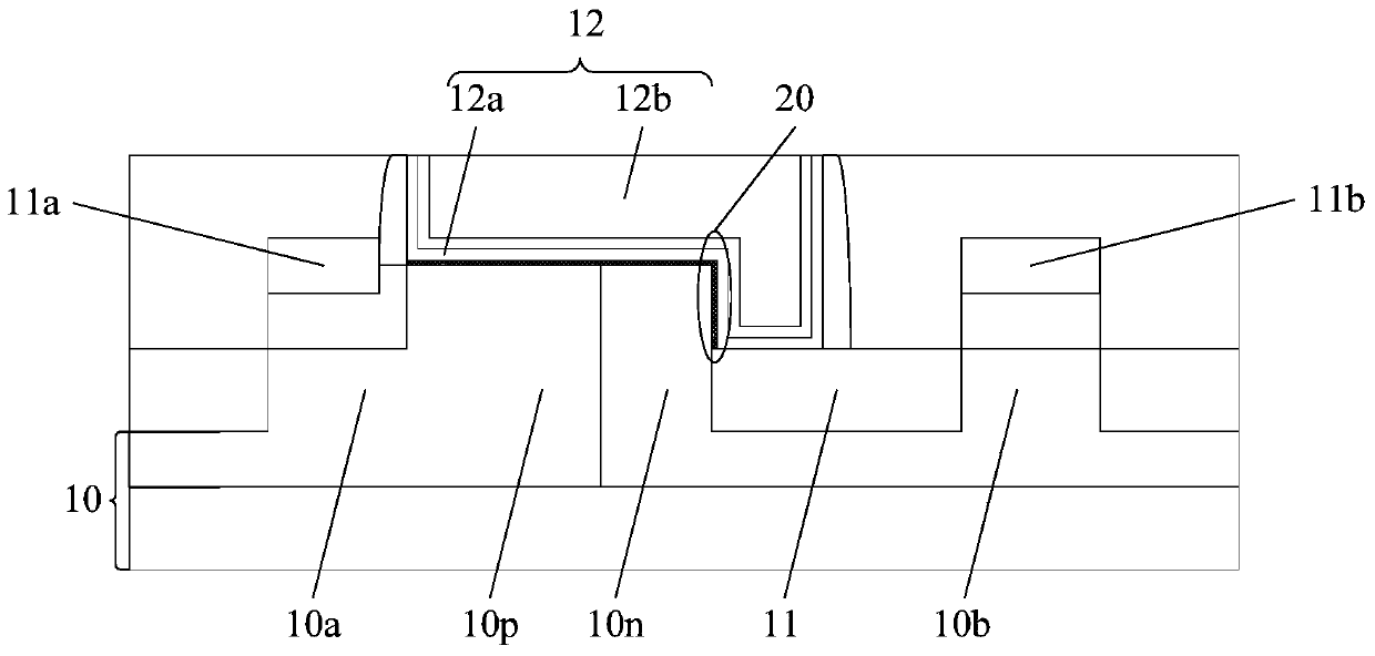
[0036] It can be seen from the background art that the LDMOS in the prior art has the problem that the gate dielectric layer is easily broken down. Now combined with the structure of LDMOS in the prior art, the reason why the gate dielectric layer is easy to be broken down is analyzed:

[0037] refer to figure 1 , shows a schematic structural diagram of an LDMOS in the prior art.

[0038] Such as figure 1 shown, the LDMOS includes:

[0039] The adjacent P-type well region 10p and N-type well region 10n are formed in the substrate 10; the isolation structure 11 located in the N-type region, the top surface of the isolation structure 11 is lower than the P-type well region 10p and the The top surface of the N-type well region 10n; the gate structure 12 located on the surface of the substrate 10, the gate structure 12 covering the top of the P-type well region 10p, the top and side walls of the N-type well region 10n, and part of the surface of the top of the isolation structu...


PUM


Abstract

The invention discloses a formation method of a transistor. The formation method comprises the following steps: forming a substrate, wherein a first well region and a second well region which are adjacent are formed in the substrate; forming an isolation structure in the second well region, wherein the top surface of the isolation structure is lower than the top surface of the first well region and the top surface of the second well region; forming a pseudo grid structure on the substrate; forming a source region or a drain region respectively in second regions of the first well region and the second well region in which the pseudo grid structure is exposed; forming a dielectric layer; forming an opening in the dielectric layer; forming grid dielectric layers on the bottom and the side wall of the opening; forming work function layers on the dielectric layers; carrying out ion injection treatment so as to adjust work functions of the work function layers; and forming grid electrodes. After the step of forming the work function layers and before the step of forming the grid electrodes, the ion injection treatment is carried out on the work function layers so as to adjust the work functions of the work function layers, so that the problem that the threshold voltage distribution of the transistor is non-uniform is solved, the punch-through of the grid dielectric layers is reduced, and the performance of the formed transistor is improved.

Description

technical field [0001] The invention relates to the field of semiconductor manufacturing, in particular to a method for forming a transistor. Background technique [0002] Laterally Diffused Metal Oxide Semiconductor (LDMOS) is a commonly used high-voltage device. [0003] LDMOS is widely adopted due to its easier compatibility with CMOS processes. LDMOS is a power device with a double-diffusion structure. Two implants are performed in the same source region or drain region, one with a higher concentration of arsenic ions and the other with a lower concentration of boron ions. After implantation, a high-temperature push process is performed. Since boron ions diffuse faster than arsenic ions, boron ions will diffuse farther below the gate boundary along the lateral direction, thereby forming a channel with a concentration gradient. The length of the LDMOS channel is determined by the difference between the two lateral diffusion distances. [0004] In order to improve the w...

Claims


Application Information

Patent Timeline
Patent Type & Authority Patents(China)
IPC IPC(8): H01L21/336H01L21/28H01L29/78
CPCH01L21/2822H01L29/66681H01L29/7816
Inventor 周飞
Owner SEMICON MFG INT (SHANGHAI) CORP
Why Eureka
Try Eureka