Process method for improving interlayer alignment accuracy in multilayer co-fired ceramic circuit processing

A technology for circuit processing and alignment accuracy, which is applied in multi-layer circuit manufacturing, printed circuit, circuit substrate materials, etc., which can solve the problem of ensuring precise control of thickness uniformity, decreased interlayer alignment accuracy, and lack of wide applicability, etc. problem, to achieve the effect of versatility, increased interlayer stability, and good dimensional stability

Active Publication Date: 2017-08-15
SOUTHWEST CHINA RES INST OF ELECTRONICS EQUIP
View PDF3 Cites 1 Cited by
  • Summary
  • Abstract
  • Description
  • Claims
  • Application Information

AI Technical Summary

Problems solved by technology

[0005] First of all, for circuit substrates with complex cavity structures and high through-hole / wiring density, due to the poor structural strength of the local multi-cavity / porous regions of green ceramics, only a few points are used to fix them, and local deformation will easily occur after lamination. Moreover, during the process of product transfer, vacuum packaging, etc., the layers are loose, and local sliding dislocations are prone to occur, which will lead to a decrease in the alignment accuracy between the layers of the product as a whole or in a local area.
Secondly, the green porcelain system with better high-temperature viscosity has the advantage of high-temperature viscosity, but this function depends on the effective deployment of green porcelain formula, which does not have wide applicability, and the existing commercial lamination equipment is the function of point heating In order to improve the fixity between green porcelain layers, if spot welding is changed to surface welding, it means higher equipment modification costs; and for green porcelain systems with poor high-temperature viscosity, if local point bonding of glue is simply changed to Glue bonding for the entire surface will not only greatly increase the cumbersome lamination workload, but also it is difficult to ensure precise control of thickness and uniformity of the entire area for surface coating of glue, which will easily lead to delamination such as substrate sintering, Distortion and other problems, or the incompatibility of the glue and green porcelain sintering will cause the electrical properties of the substrate to deviate

Method used


Image

  • Process method for improving interlayer alignment accuracy in multilayer co-fired ceramic circuit processing
  • Process method for improving interlayer alignment accuracy in multilayer co-fired ceramic circuit processing
  • Process method for improving interlayer alignment accuracy in multilayer co-fired ceramic circuit processing

Examples


Embodiment 1

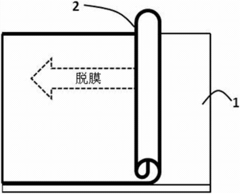
[0046] 1) After the raw porcelain is cut into the standard process size, tear off the Mylar film 2 that comes with the raw porcelain from the green porcelain 1, as shown in figure 1 shown.

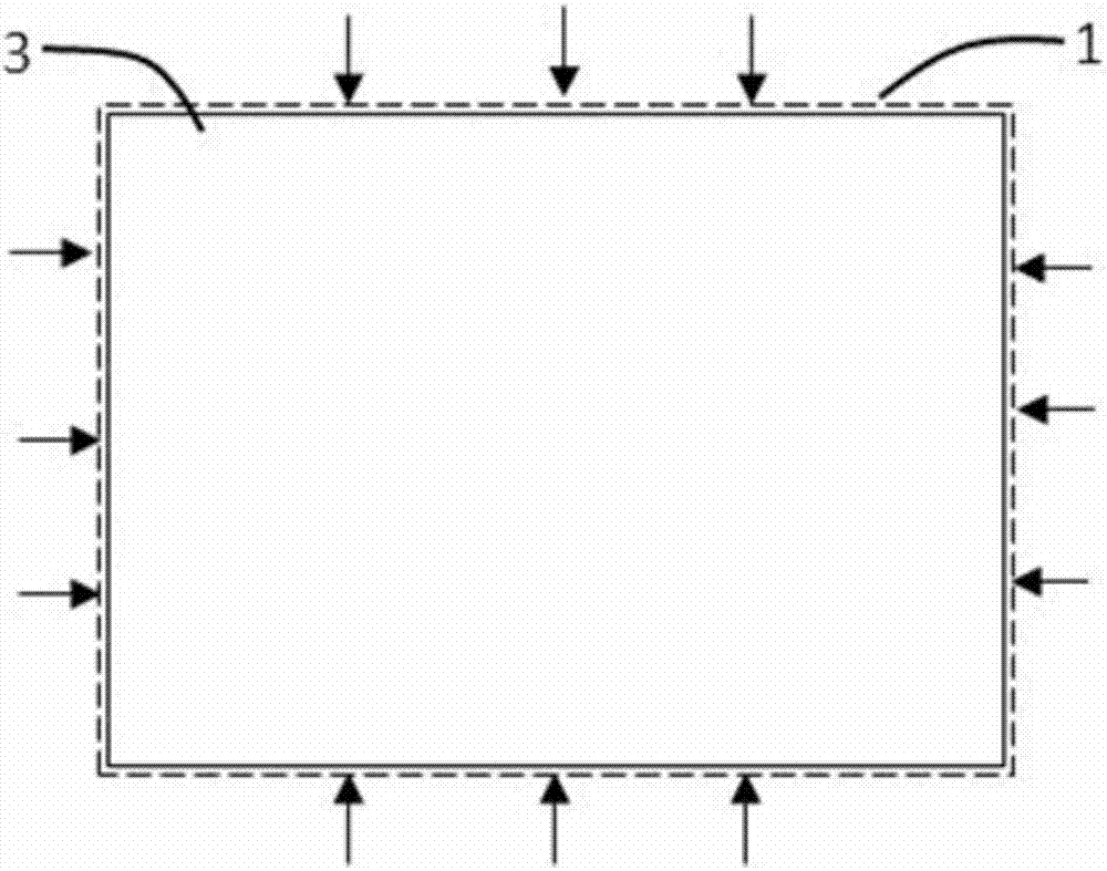
[0047] 2) Dry the green porcelain 1 without film at 60°C for 30 minutes to obtain green porcelain 3 with proper deformation, such as figure 2 shown.

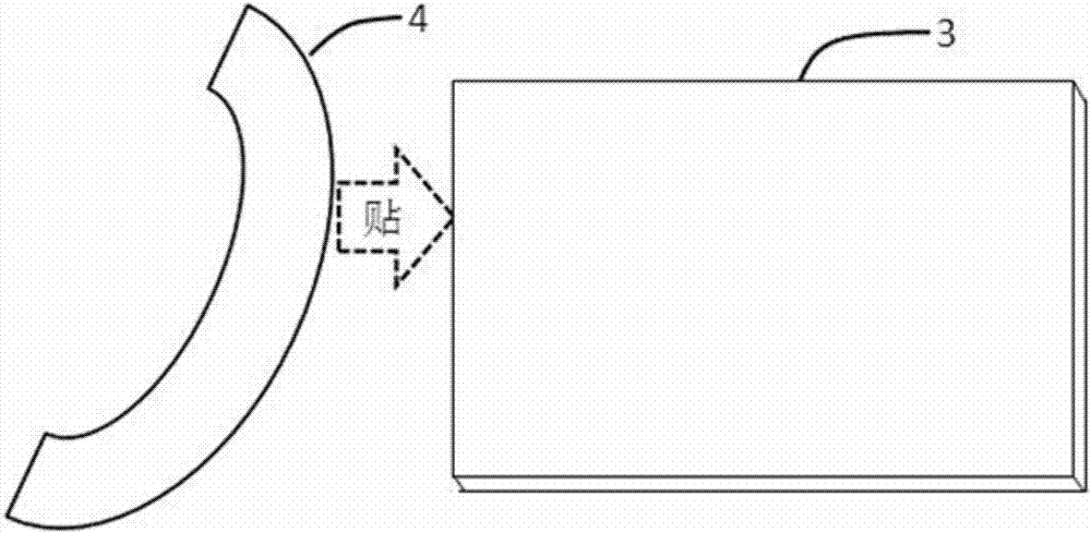
[0048] 3) Paste the organic film 4 coated with a 1 μm low-viscosity coating on one side on the deformed green porcelain 3, as shown in image 3 shown. The thickness of the organic membrane 4 is 50 μm.

[0049] 4) The raw porcelain after the second film is like Figure 4 As shown, the green ceramic 3 and the organic film 4 are well bonded, and the green ceramic can maintain a low amount of deformation during the process of multilayer co-fired ceramic circuits.

[0050] 5) The processing is completed by conventional multi-layer ceramic circuit processes such as punching, filling, printing, stripping, and lamination.

Embodiment 2

[0052] 1) After the raw porcelain is cut into the standard process size, tear off the Mylar film 2 that comes with the raw porcelain from the green porcelain 1, as shown in figure 1 shown.

[0053] 2) The green porcelain 1 without film is placed naturally in a 100,000-class purification environment for 8 hours to obtain green porcelain 3 with proper deformation, such as figure 2 shown.

[0054] 3) Paste the organic diaphragm 4 coated with a 2.5 μm low-viscosity coating on one side on the deformed raw porcelain 3, as shown in image 3 shown. The thickness of the organic membrane 4 is 75 μm.

[0055] 4) The raw porcelain after the second film is like Figure 4 As shown, the green ceramic 3 and the organic film 4 are well bonded, and the green ceramic can maintain a low amount of deformation during the process of multilayer co-fired ceramic circuits.

[0056] 5) The conventional multilayer ceramic circuit technology of punching, hole filling, printing, stripping, lamination...

Embodiment 3

[0066] 1) Tear off the Mylar film A-2 of the original green porcelain A from the green porcelain A-1, and then stick the organic film B coated with the adhesive coating B-1 on a hot stage at 40°C On the back of the green porcelain, the bonding coating is in contact with the back of the green porcelain to form a new structure C. see Figure 5-7 .

[0067] 2) Fabricate through holes 1-1, conductor patterns 1-2, and cavities 1-3 in the first layer of the product on structure C using conventional processes. J-1 is a through hole for optical alignment, and J-2 is an alignment hole for pin stacking, such as Figure 8 shown.

[0068] 3) According to the method in 2), the processing of each layer of raw porcelain except the last layer is completed on the new structure C, such as Figure 9-10 shown.

[0069] 4) Use the conventional process to complete the through hole L-1, the conductor pattern L-2, the through hole J-1 for optical alignment, and the alignment hole J-2 for pin lam...


PUM

PropertyMeasurementUnit
thicknessaaaaaaaaaa
thicknessaaaaaaaaaa
thicknessaaaaaaaaaa

Abstract

The invention discloses a process method for improving interlayer alignment accuracy in multilayer co-fired ceramic circuit processing. The process method comprises a step of inhibiting deformation of raw ceramic and a step of coating with an adhesive coating before lamination. The step of inhibiting deformation of the raw ceramic comprises: firstly, carrying out demoulding and aging on the raw ceramic, then carrying out secondary lamination on the aged raw ceramic, eliminating a residual stress between a film and the raw ceramic, and reducing a deformation quantity to below 0.03% from conventional over 0.06%; the step of coating with the adhesive coating before lamination comprises the following steps: before the raw ceramic is laminated, coating the raw ceramic with one layer of adhesive coating on a hot plate with a temperature of 35 DEG C to 50 DEG C, implementing adhering of adjacent layers of raw ceramic after lamination, integrally fixing each layer of raw ceramic, and then proceeding a subsequent process. The adhesive coating can be decomposed and discharged at a temperature interval of 400 to 600 DEG C, does not interfere performance of a circuit substrate and has excellent compatibility. The process method disclosed by the invention has the advantages of low cost, wide application range and convenience in use; interlayer alignment accuracy of the circuit substrate can be effectively improved; alignment accuracy is below 30mu m.

Description

technical field [0001] The invention belongs to the field of multilayer co-fired ceramic circuit processing, and specifically relates to a process method for improving interlayer alignment accuracy in multilayer co-fired ceramic circuit processing. Alignment accuracy. Background technique [0002] The multi-layer co-fired ceramic circuit represented by LTCC (low temperature co-fired ceramic) has outstanding advantages such as high integration density, microwave / digital / control multi-functional hybrid integration, excellent high-frequency performance, etc., and has gradually become a miniaturized, high-performance T It is the first choice to implement circuit substrates such as / R components, frequency sources, and phased array antennas, and has been widely used in aviation, aerospace, missile-borne, ship-borne and other fields. [0003] The conventional production process of multi-layer co-fired ceramic circuit boards is: raw porcelain cutting→green porcelain drilling→green...

Claims


Application Information

Patent Timeline
Patent Type & Authority Applications(China)
IPC IPC(8): H05K3/46H05K1/02H05K1/03
CPCH05K1/0271H05K1/0306H05K3/4638
Inventor 岳帅旗刘志辉王娜
Owner SOUTHWEST CHINA RES INST OF ELECTRONICS EQUIP
Why Eureka
Try Eureka