Broad spectrum displayer covering visible light to infrared wave band

An infrared band, wide spectrum technology, applied in the field of display technology and metal nanomaterials, can solve the problems of slow response speed of electrowetting multicolor display, unable to dynamically tune spectrum, easy degradation of color ink, etc., and achieve poor stability and service life. Long, short duration effect

Active Publication Date: 2017-08-18
SOUTHEAST UNIV
4 Cites 0 Cited by

AI-Extracted Technical Summary

Problems solved by technology

[0007] Technical problem: The purpose of the present invention is to solve the problem that the color ink used in the existing electrowetting display is easy to degrade under long-term light conditions, has poor stability, cannot d...

Method used

[0038] The wide-spectrum display covering visible light to infrared bands of the present invention is based on the principle of electrowetting and the LSPR effect of plasmonic nanoparticles, and can realize dynamic tuning of the scattering spectrum of plasmonic nanoparticles. First, when no voltage is applied between the first electrode and the second electrode, the local surface plasmon resonance of the nanoparticle film at the two-phase interface is not obvious, and the color of the nanoparticle is reflected at this time; when passed The peripheral driving circuit applies a voltage to change the interfacial tension between the first liquid, the second liquid and the dielectric layer, and then change the hydrophobic angle of the second liquid, so that the coverage area of ​​the second liquid on the dielectric layer changes, resulting in self-assembly in the The distance between the nanoparticles at the interface between the first liquid and the second liquid changes; using the LSPR effect of the nanoparticles, when the distance between the nanoparticles changes, the scattering spectrum will be blue-shifted or re...

Abstract

The invention discloses a broad spectrum displayer covering visible light to an infrared band. The broadband spectrum displayer covering the visible light to the infrared band consists of an array of display units; the display unit comprises a second electrode (9), a hydrophobic insulating layer (8), a fluid chamber (2), a blocking layer (6), a medium layer (5), a first electrode (4), a substrate (3) and an illumination layer (14) which are successively arranged from the top to the bottom; and the two ends of a periphery driving circuit (13) are respectively connected to the first electrode (4) and the second electrode (9). The broad spectrum displayer covering the visible light to the infrared band uses a localized surface Plasmon resonance effect of Plasmon nanometer particles. When distance between nanometer particles changes, a spectral peak of a spectrum can move so as to change the color of a display unit and realize the dynamic tuning of the spectrum. The broadband spectrum displayer can fast respond, can be used as a micro-displayer to be applied to an anti-fake label and can realize flexible display, and is low in cost and simple in manufacture technology.

Application Domain

Technology Topic

Image

  • Broad spectrum displayer covering visible light to infrared wave band
  • Broad spectrum displayer covering visible light to infrared wave band
  • Broad spectrum displayer covering visible light to infrared wave band

Examples

  • Experimental program(1)

Example Embodiment

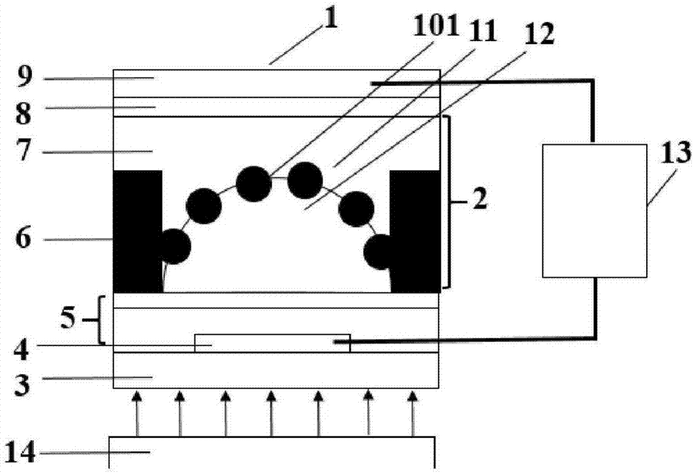
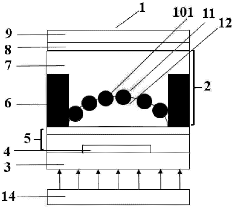
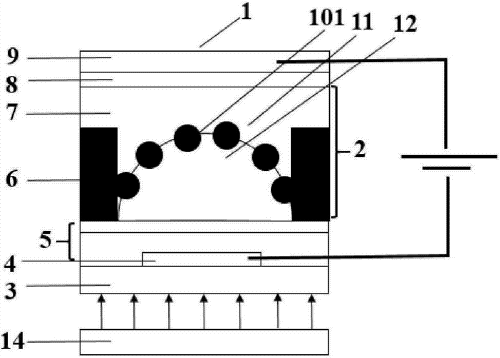
[0035] A wide-spectrum display covering the visible light to infrared bands of the present invention is composed of arrayed display units. The display is composed of arrayed display units. Each display unit 1 may contain a single sub-display unit 16, or It may contain multiple sub-display units. The display unit 1 includes: a fluid chamber 2, a substrate 3, a first electrode 4, a dielectric layer 5, a barrier layer 6, a first liquid 7, a hydrophobic insulating layer 8, a second electrode 9, a plasma The excimer nano-film 11, the second liquid 12, the peripheral driving circuit 13 and the illumination layer 14. The positional relationship from top to bottom is the second electrode 9, the hydrophobic insulating layer 8, the fluid chamber 2, the barrier layer 6, the dielectric layer 5, the first electrode 4, the substrate 3, the illuminating layer 14, and the connecting first electrode 4 and The peripheral driving circuit 13 of the second electrode 9.
[0036] The fluid chamber 2 is composed of a first liquid 7, a second liquid 12 and a plasmon nano film 11. The plasmonic nano-film 11 is self-assembled by plasmonic nanoparticles 101 at the interface of the first liquid 7 and the second liquid 12. The first liquid 7 and the second liquid 12 are not miscible or slightly soluble.
[0037] The display unit 1 is based on the principle of electrowetting, and a voltage is applied between the first electrode 4 and the second electrode 9 through the peripheral drive circuit 13 to change the interfacial tension between the first liquid 7, the second liquid 12 and the dielectric layer 5. , Thereby changing the hydrophobic angle of the second liquid 12, so that the coverage area of ​​the second liquid 12 on the dielectric layer 5 changes, resulting in the self-assembled plasmonic nanoparticles 101 at the interface of the first liquid 7 and the second liquid 12 The spacing varies from 1 nanometer to 300 nanometers; using the local plasmon resonance effect of plasmon nanoparticles 101, when the spacing of plasmon nanoparticles 101 becomes smaller, the peak of its scattering spectrum will be red-shifted; When the distance between the plasmon nanoparticles 101 becomes larger, the peak of the scattering spectrum is blue-shifted, which realizes the dynamic tunability of the scattering spectrum of the plasmon nanoparticles and changes the color of the display unit.
[0038] The wide-spectrum display covering the visible light to infrared band of the present invention is based on the principle of electrowetting and the LSPR effect of plasmon nanoparticles, and can realize dynamic tuning of the scattering spectrum of plasmon nanoparticles. First, when no voltage is applied between the first electrode and the second electrode, the local surface plasmon resonance of the nanoparticle film at the two-phase interface is not obvious, and the color of the nanoparticle is reflected at this time; The peripheral driving circuit applies a voltage to change the interfacial tension between the first liquid, the second liquid and the dielectric layer, thereby changing the hydrophobic angle of the second liquid, so that the coverage area of ​​the second liquid on the dielectric layer changes, resulting in self-assembly in The distance between the nanoparticles at the interface of the first liquid and the second liquid is changed; using the LSPR effect of the nanoparticles, when the distance between the nanoparticles is changed, the scattering spectrum will be blue-shifted or red-shifted, realizing a new type of display with dynamically tunable spectrum. Second, the display unit can contain a single sub-display unit or multiple sub-display units. Since the nano-films formed by the self-assembly of different types and shapes of nanoparticles will show different colors, and the change of the nanoparticle spacing can also tune the spectrum, the display can use different types and different morphologies of plasmon nanoparticles With different SPR peaks, by changing the spacing of the nanoparticles, the spectrum adjustment range of the display is expanded. Third, the display unit is based on the mechanism of electrowetting and the LSPR effect of metal nanoparticles, and can adopt a single-layer or multi-layer structure to realize the color control of the display unit. Due to the LSPR effect of metal nanoparticles, the color seen by the naked eye of metal nanoparticles of the same type and morphology is different from the color seen under a microscope. The two colors are complementary colors, which can be used as microdisplays and used in anti-counterfeiting signs. .
[0039] The present invention is further illustrated by specific examples and comparative examples below:
[0040] The M×N array structure is prepared, and transparent electrodes are prepared on the substrate by photolithography, etching and other processes, and then the dielectric layer is prepared by ALD above, and the low surface stress polymer dielectric layer is prepared by the spin coating process. Subsequently, an M×N grid layer is prepared by nanoimprinting technology to form an array chamber structure, and the hydrophilic material of the spacer layer is generally a hydrophilic polymer material such as polyethylene glycol and polyacrylamide. The metal nanoparticles treated with surface ligands are self-assembled at the interface of the first liquid and the second liquid and then filled into the fluid chamber.
[0041] The prepared display unit array is connected to the peripheral driving circuit through the bottom electrode and the top electrode, and the display unit is controlled by the digital signal of the driving circuit.
[0042] After the preparation of a single display unit is completed, follow the above steps to continue to prepare multiple display units. Such repetition finally obtains a large-scale display unit array as a display device.
[0043] In addition, those skilled in the art can make other changes within the spirit of the present invention. Of course, these changes made in accordance with the spirit of the present invention should all be included in the scope of protection claimed by the present invention.

PUM

PropertyMeasurementUnit
Size1000.0nm
Thickness50.0 ~ 300.0nm
Thickness300.0 ~ 800.0nm
tensileMPa
Particle sizePa
strength10

Description & Claims & Application Information

We can also present the details of the Description, Claims and Application information to help users get a comprehensive understanding of the technical details of the patent, such as background art, summary of invention, brief description of drawings, description of embodiments, and other original content. On the other hand, users can also determine the specific scope of protection of the technology through the list of claims; as well as understand the changes in the life cycle of the technology with the presentation of the patent timeline. Login to view more.

Similar technology patents

Ink jet recording material

ActiveUS20120148767A1Easily available and safetyPoor stabilityDuplicating/marking methodsCoatingsPolymer chemistryPigment
Owner:MITSUBISHI PAPER MILLS LTD

Aloe-containing hangover-alleviating beverage

InactiveCN107137565ADifficult to extractPoor stabilityDigestive systemAntinoxious agentsBacteriostatic agentStart time
Owner:HUBEI UNIV FOR NATITIES

Wind power generation high-power flexible long-range transmission device

ActiveCN105156283AHigh reliability requirementsPoor stabilityWind energy generationWind motor componentsWind forceElectricity
Owner:LANZHOU UNIVERSITY OF TECHNOLOGY

Method for recycling transparent conductive electrode of organic solar cell

ActiveCN110797464ALow photoelectric conversion efficiencyPoor stabilityWaste processingTransportation and packagingElectrically conductiveMetallic electrode
Owner:CHONGQING UNIV OF ARTS & SCI +1

Classification and recommendation of technical efficacy words

  • Poor stability
  • Short use time

Wireless monitoring bio-diagnosis system

InactiveUS20100274101A1Poor stabilityMicrobiological testing/measurementCatheterMedical unitEngineering
Owner:NAT TAIWAN UNIV

Fabrication method for an in-stack stabilized synthetic stitched CPP GMR head

InactiveUS20050219773A1Poor stabilityEnhance exchangeNanostructure applicationNanomagnetismLower fieldMagnetic layer
Owner:HEADWAY TECH INC

Arrangement for Obtaining Reliable Anchoring of a Threaded Implant in a Bone

InactiveUS20150044639A1Poor stabilityCut geometry of becomes badDental implantsBone implantBiomedical engineeringRotational stability
Owner:NOBEL BIOCARE SERVICES AG

Stable transmission machine

Owner:山东雪莱粮仓智能科技有限公司

Facial mask

InactiveCN106551890AShort use timeQuick resultsCosmetic preparationsToilet preparationsImidazolidinyl ureaGlycerol
Owner:无锡市汉方八珍科技有限公司

Heavy-industry machine platform

Owner:SUZHOU INST OF TRADE & COMMERCE
Why Eureka
Try Eureka