Transferable patterned conductive thin film structure and patterning method thereof

A conductive thin film and transfer pattern technology, applied to the conductive layer, circuit, electrical components and other directions on the insulating carrier, can solve the problem of poor adhesion between nano-metal materials and substrates

Active Publication Date: 2017-08-25
SUN YAT SEN UNIV
View PDF17 Cites 5 Cited by
  • Summary
  • Abstract
  • Description
  • Claims
  • Application Information

AI Technical Summary

Problems solved by technology

In the overall conductive film structure, because of the addition of an adhesion-enhancing layer, the nano-metal material on the conductive layer can be firmly fixed, which solves the problem of poor adhesion between the nano-metal material and the substrate; especially in the patterning process , to prevent th...

Method used


Image

  • Transferable patterned conductive thin film structure and patterning method thereof
  • Transferable patterned conductive thin film structure and patterning method thereof
  • Transferable patterned conductive thin film structure and patterning method thereof

Examples


Embodiment 1

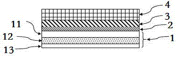
[0054] The structure of the transferable patterned conductive film is shown in the attached figure 1 As shown, a release film, an adhesive layer, a flexible substrate, an adhesion enhancement layer, a conductive layer and a photosensitive film layer are stacked sequentially from bottom to top.

Embodiment 2

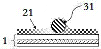
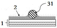
[0056] The general preparation method of transferable patterned conductive film is to first prepare conductive ink, which is specifically composed of polymer molecules, nano-metal materials, and solvents, and then attached to a flexible substrate. figure 2 As shown, a composite layer of the polymer layer and the nano-metal material is formed at this time, and then by adding a cross-linking agent to the polymer layer, the cross-linking agent reacts with the polymer molecules in the polymer layer to form an adhesion-enhancing layer, that is attached image 3 shown. Finally, the prepared photosensitive film layer is attached to the conductive layer to complete the preparation of the transferable patterned conductive film.

Embodiment 3

[0058] The patterning method of the transferable patterned conductive film is as follows: first, exposure is performed according to the set pattern, and after the exposure is completed, it is developed by a developer. At this time, the unexposed photosensitive adhesive layer still exists, and the exposed photosensitive adhesive layer still exists. The adhesive layer is completely removed to expose the conductive layer. At this time, the etching process is performed again, and the etching solution will corrode the exposed conductive layer. After the etching is completed, a glue removal process is performed. After the glue removal is completed, the patterning of the conductive layer is completed. Finally, when it is necessary to transfer the patterned conductive film, it is only necessary to tear off the release film and combine the adhesive layer with the target substrate. Figure 4 And attached Figure 5 shown, it is done. (Whether to add examples to make photosensitive dry...


PUM

PropertyMeasurementUnit
The average diameteraaaaaaaaaa
Resistanceaaaaaaaaaa

Abstract

The invention discloses a transferable patterned conductive thin film structure and a patterning method thereof. An adhesion enhancement layer, a conductive layer and a photosensitive film layer are formed on a transfer substrate, patterning processing is performed in the case of ensuring connection stability between the conductive layer and the substrate to form a transferable conductive pattern, and finally, the conductive pattern can be transferred to a target substrate through the transfer substrate. The conductive thin film structure of the invention provides a high stability transferable conductive pattern compatible with large area mass production, provides a solution for special shape, curved and stick-on electronic devices, and has high application prospects.

Description

technical field [0001] The invention relates to the field of conductive thin films, in particular to a transferable patterned conductive thin film and a method for preparing and patterning the same. Background technique [0002] At present, in the age of electronic information, many electronic devices have penetrated into people's lives, and large-scale, flexible, bendable, and transferable electronic devices are the general trend of the development of electronic devices. Electronic touch screens are typical representatives of these electronic devices; Undoubtedly, a touch screen that satisfies the above characteristics requires a conductive film that can be patterned and transferred arbitrarily. Moreover, on the basis of ensuring the properties of the film, the manufacturing process we hope to achieve must be simple, low-cost, and environmentally friendly at the same time. production and sustainability requirements. Since the discovery of ITO material, its superior electro...

Claims


Application Information

Patent Timeline
IPC IPC(8): H01B5/14H01B13/00
CPCH01B5/14H01B13/00
Inventor 杨柏儒许钰旺刘贵师
Owner SUN YAT SEN UNIV
Why Eureka
Try Eureka