WSiAlN thin film for piezoelectric thin film transducer and preparation method thereof

A piezoelectric thin film, transducer technology, applied to the manufacture/assembly of piezoelectric/electrostrictive devices, piezoelectric/electrostrictive/magnetostrictive devices, materials for piezoelectric devices or electrostrictive devices Choosing the same direction can solve the problems of poor c-axis orientation, large stress, and difficult control of W film stress, and achieve the effect of improving c-axis orientation, reducing stress, and reducing stress

Active Publication Date: 2017-08-25
CHINA ELECTRONICS TECH GRP NO 26 RES INST
View PDF4 Cites 0 Cited by
  • Summary
  • Abstract
  • Description
  • Claims
  • Application Information

AI Technical Summary

Problems solved by technology

[0003] The invention provides a WSiAlN thin film for a piezoelectric thin film transducer and a preparation method thereof to solve the problem that tungsten W is used as the bottom electrode at present, the stress of the W thin film is not easy to control, and the piezoelectric thin film grown on it has poor c-axis orientation. stressful problems

Method used


Image

  • WSiAlN thin film for piezoelectric thin film transducer and preparation method thereof
  • WSiAlN thin film for piezoelectric thin film transducer and preparation method thereof
  • WSiAlN thin film for piezoelectric thin film transducer and preparation method thereof

Examples


preparation example Construction

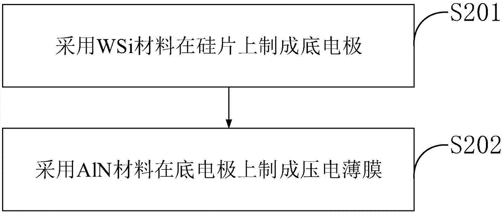
[0034] In addition, the present invention also provides a preparation method of a WSiAlN thin film for a piezoelectric thin film transducer, such as figure 2 As shown, it may include the following steps:

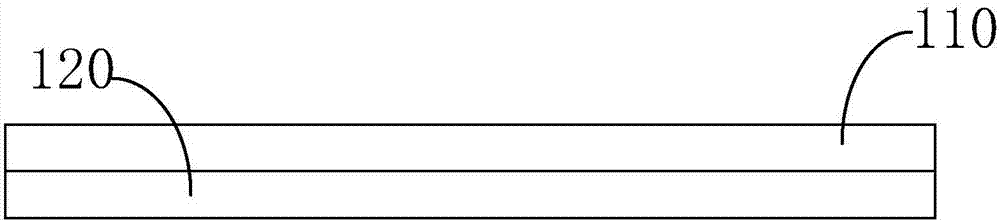
[0035] Step S201 , using WSi material to form a bottom electrode on a silicon wafer.

[0036] In this embodiment, the molar ratio of W and Si in the WSi material is 1:2˜1:2.7, thereby ensuring that the c-axis orientation of the piezoelectric film is improved and its stress is reduced. Wherein, the use of WSi material to form the bottom electrode on the silicon wafer may include:

[0037]The bottom electrode is made of WSi material on the silicon wafer by DC magnetron sputtering, wherein the manufacturing process parameters of DC magnetron sputtering are: sputtering power 2000-4000W, argon flow rate 35-55sccm, back argon flow rate 15sccm. The present invention prepares the WSi bottom electrode by means of DC magnetron sputtering, which can ensure that the resistivity of th...
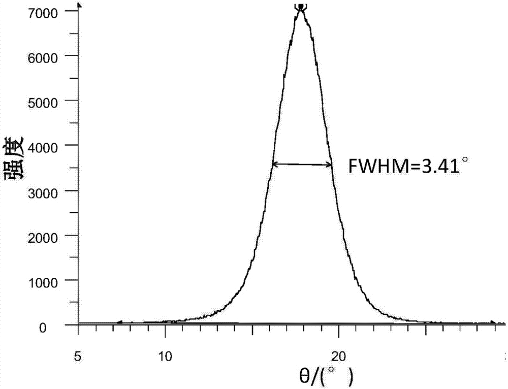
Embodiment 1

[0044] 1) The WSi bottom electrode is manufactured on the silicon wafer by DC magnetron sputtering, the manufacturing process: the sputtering power is 2000w, the flow rate of argon gas is 35 sccm, and the flow rate of argon gas on the back is 15 sccm.

[0045] 2) Rapid annealing at a high temperature of 600°C for 30 seconds.

[0046] 3) The AlN piezoelectric film was fabricated by AC magnetron sputtering under the process conditions of sputtering power of 3000w, argon gas flow rate of 4 sccm, and nitrogen gas flow rate of 10 sccm.

[0047] 4) test the rocking curve of the AlN piezoelectric film on the sample, as image 3 shown.

[0048] 5) Test the stress of the AlN piezoelectric thin film on the sample.

[0049] 6) Test the roughness of the AlN piezoelectric thin film on the sample.

Embodiment 2

[0051] 1) The WSi bottom electrode is manufactured on the silicon wafer by DC magnetron sputtering, the manufacturing process: the sputtering power is 3000w, the flow rate of argon gas is 45 sccm, and the flow rate of argon gas on the back is 15 sccm.

[0052] 2) Rapid annealing at a high temperature of 800°C for 60 seconds.

[0053] 3) The AlN piezoelectric film was fabricated by AC magnetron sputtering under the process conditions of sputtering power of 5000w, argon gas flow rate of 8 sccm, and nitrogen gas flow rate of 20 sccm.

[0054] 4) test the rocking curve of the AlN piezoelectric film on the sample, as Figure 4 shown.

[0055] 5) Test the stress of the AlN piezoelectric thin film on the sample.

[0056] 6) Test the roughness of the AlN piezoelectric thin film on the sample.


PUM

PropertyMeasurementUnit
Stressaaaaaaaaaa
Roughnessaaaaaaaaaa

Abstract

The invention provides a WSiAlN thin film for a piezoelectric thin film transducer and a preparation method thereof. The WSiAlN thin film for the piezoelectric thin film transducer comprises a bottom electrode and a piezoelectric thin film located on the bottom electrode, wherein the bottom electrode is made of a material WSi, and the piezoelectric thin film is made of a material AlN. According to the invention, the bottom electrode is made by adopting the material WSi and arranged below the AlN piezoelectric thin film, so that the c-axis orientation of the piezoelectric thin film can be improved, the stress is reduced, and requirements of a composite thin film material for the piezoelectric thin film transducer are met. The composite thin film material structural unit provided by the invention, namely, the WSiAlN thin film, can act as a novel thin film material structural unit to use in the piezoelectric thin film transducer.

Description

technical field [0001] The invention belongs to the field of piezoelectric film transducers, which are core components of bulk acoustic wave devices such as film bulk acoustic wave filters and bulk acoustic wave microwave delay lines, and specifically relates to a WSiAlN film for piezoelectric film transducers and a preparation method thereof. Background technique [0002] The core part of bulk acoustic wave devices such as thin-film bulk acoustic wave devices and bulk acoustic wave microwave delay lines is the piezoelectric thin-film transducer. The bulk acoustic wave piezoelectric film transducer is composed of a bottom electrode, a piezoelectric film and an upper electrode. The bottom electrode and the piezoelectric film are the key to the manufacture of the piezoelectric film transducer. Aluminum nitride (AlN) piezoelectric thin film is the preferred material for making piezoelectric thin film transducers because of its wide band gap, high breakdown voltage, high sound v...

Claims


Application Information

Patent Timeline
IPC IPC(8): H01L41/047H01L41/29H01L41/39H01L41/18
CPCH10N30/877H10N30/85H10N30/06H10N30/093
Inventor 欧黎徐阳江洪敏司美菊姜华男张永川马晋毅龙飞杜波蒋欣金成飞田本朗
Owner CHINA ELECTRONICS TECH GRP NO 26 RES INST
Why Eureka
Try Eureka