A kind of Wsialn thin film for piezoelectric thin film transducer and preparation method thereof
A piezoelectric thin film, transducer technology, applied to the manufacture/assembly of piezoelectric/electrostrictive devices, piezoelectric/electrostrictive/magnetostrictive devices, materials for piezoelectric devices or electrostrictive devices Choosing the same direction can solve the problems of large stress, poor c-axis orientation, and difficult control of W film stress, and achieve the effects of reducing stress, improving c-axis orientation, and reducing stress
- Summary
- Abstract
- Description
- Claims
- Application Information
AI Technical Summary
Problems solved by technology
Method used
Image
Examples
preparation example Construction
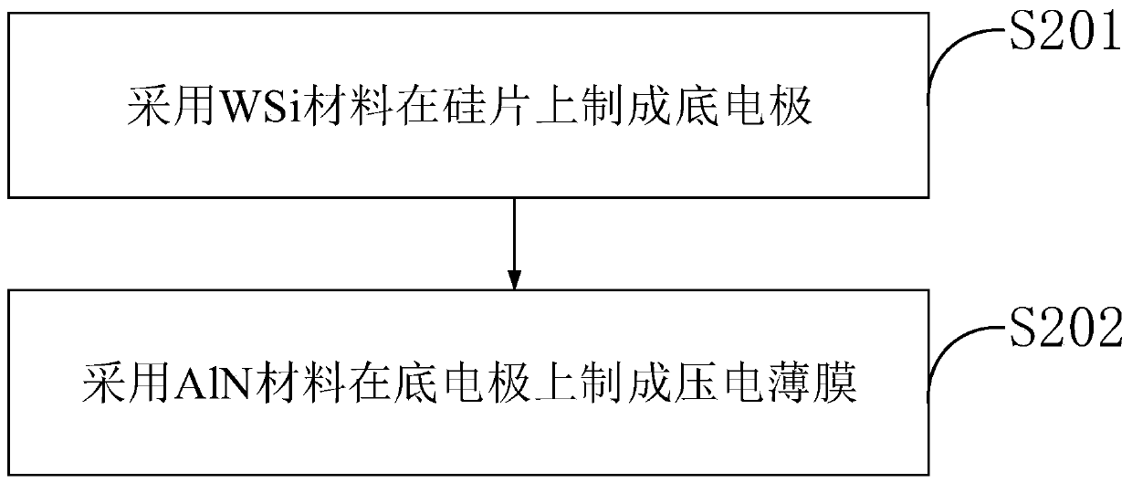
[0034] In addition, the present invention also provides a preparation method of a WSiAlN thin film for a piezoelectric thin film transducer, such as figure 2 As shown, it may include the following steps:
[0035] Step S201 , using WSi material to form a bottom electrode on a silicon wafer.
[0036] In this embodiment, the molar ratio of W and Si in the WSi material is 1:2˜1:2.7, thereby ensuring that the c-axis orientation of the piezoelectric film is improved and its stress is reduced. Wherein, the use of WSi material to form the bottom electrode on the silicon wafer may include:
[0037]The bottom electrode is made of WSi material on the silicon wafer by DC magnetron sputtering, wherein the manufacturing process parameters of DC magnetron sputtering are: sputtering power 2000-4000W, argon flow rate 35-55sccm, back argon flow rate 15sccm. The present invention prepares the WSi bottom electrode by means of DC magnetron sputtering, which can ensure that the resistivity of th...
Embodiment 1
[0044] 1) The WSi bottom electrode is manufactured on the silicon wafer by DC magnetron sputtering, the manufacturing process: the sputtering power is 2000w, the flow rate of argon gas is 35 sccm, and the flow rate of argon gas on the back is 15 sccm.
[0045] 2) Rapid annealing at a high temperature of 600°C for 30 seconds.
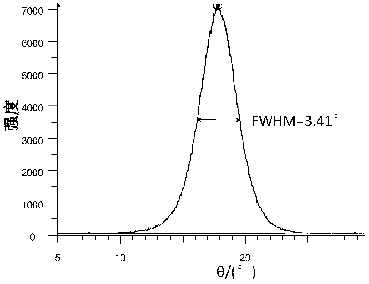
[0046] 3) The AlN piezoelectric film was fabricated by AC magnetron sputtering under the process conditions of sputtering power of 3000w, argon gas flow rate of 4 sccm, and nitrogen gas flow rate of 10 sccm.
[0047] 4) test the rocking curve of the AlN piezoelectric film on the sample, as image 3 shown.
[0048] 5) Test the stress of the AlN piezoelectric thin film on the sample.
[0049] 6) Test the roughness of the AlN piezoelectric thin film on the sample.
Embodiment 2
[0051] 1) The WSi bottom electrode is manufactured on the silicon wafer by DC magnetron sputtering, the manufacturing process: the sputtering power is 3000w, the flow rate of argon gas is 45 sccm, and the flow rate of argon gas on the back is 15 sccm.
[0052] 2) Rapid annealing at a high temperature of 800°C for 60 seconds.
[0053] 3) The AlN piezoelectric film was fabricated by AC magnetron sputtering under the process conditions of sputtering power of 5000w, argon gas flow rate of 8 sccm, and nitrogen gas flow rate of 20 sccm.
[0054] 4) test the rocking curve of the AlN piezoelectric film on the sample, as Figure 4 shown.
[0055] 5) Test the stress of the AlN piezoelectric thin film on the sample.
[0056] 6) Test the roughness of the AlN piezoelectric thin film on the sample.
PUM
| Property | Measurement | Unit |
|---|---|---|
| electrical resistivity | aaaaa | aaaaa |
Abstract
Description
Claims
Application Information


