Array substrate, driving method thereof, organic light-emitting display panel, and display device

A technology for array substrates and light-emitting devices, applied in static indicators, instruments, etc., can solve the problems of abnormal display, influence on display stability, drift of driving transistor characteristics, etc., and achieve the effect of improving stability

Active Publication Date: 2020-07-03
WUHAN TIANMA MICRO ELECTRONICS CO LTD
View PDF10 Cites 0 Cited by
  • Summary
  • Abstract
  • Description
  • Claims
  • Application Information

AI Technical Summary

Problems solved by technology

[0004] Embodiments of the present invention provide an array substrate, a driving method thereof, an organic light-emitting display panel, and a display device, which are used to solve the problem of characteristic drift of the driving transistor caused by the source of the driving transistor being under the same bias voltage for a long time in the prior art, resulting in Display abnormalities and problems affecting the stability of the display

Method used


Image

  • Array substrate, driving method thereof, organic light-emitting display panel, and display device
  • Array substrate, driving method thereof, organic light-emitting display panel, and display device
  • Array substrate, driving method thereof, organic light-emitting display panel, and display device

Examples


Embodiment 1

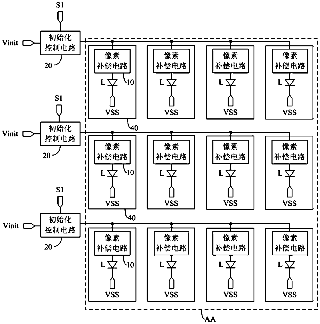
[0124] Figure 5a Each pixel unit 40 includes a pixel compensation circuit and a voltage control circuit, that is, each pixel unit 40 includes 3 transistors and 2 capacitors. To Figure 5a The structure of the circuit in the pixel unit 40 on the left side of the array substrate shown as an example is combined with Figure 7a The timing diagram is shown for explanation. Specifically, select such as Figure 7a The shown input timing diagram has four stages: initialization stage T1, threshold compensation stage T2, data writing stage T3, and light-emitting stage T4. Among them, in the initialization phase T1 and the threshold compensation phase T2, the voltage of the signal output by the data signal terminal Data is V in , The V in Much smaller than the voltage V of the signal at the initialization signal terminal Vinit init , Namely V in init . The signal output by the data signal terminal Data at least during the data writing phase T3 is the specific gray-scale voltage V d...

Embodiment 2

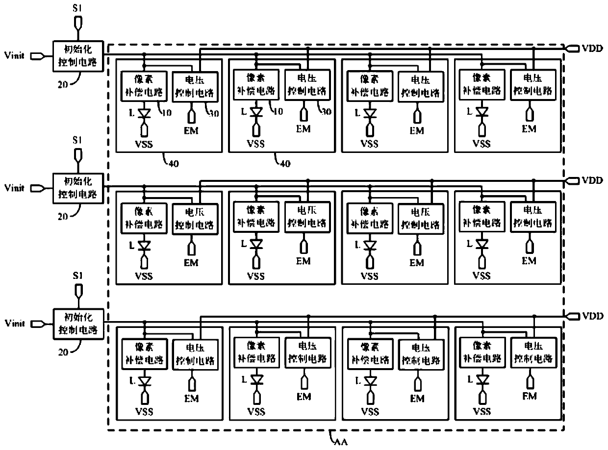
[0136] Figure 5b The pixel compensation circuits in two adjacent pixel units 40 share a voltage control circuit, that is, each pixel unit 40 includes 2.5 transistors and 2 capacitors. Among them Figure 5b The structure of the circuit in the pixel unit 40 on the left and the pixel unit 40 on the right in the array substrate shown as an example is combined Figure 7a The timing diagram is shown for explanation. Specifically, select such as Figure 7a The shown input timing diagram has four stages: initialization stage T1, threshold compensation stage T2, data writing stage T3, and light-emitting stage T4. Among them, in the initialization phase T1 and the threshold compensation phase T2, the voltage of the signal output by the data signal terminal Data is V in , The V in Much smaller than the voltage V of the signal at the initialization signal terminal Vinit init , Namely V in init . The signal output by the data signal terminal Data at least during the data writing phase...

Embodiment 3

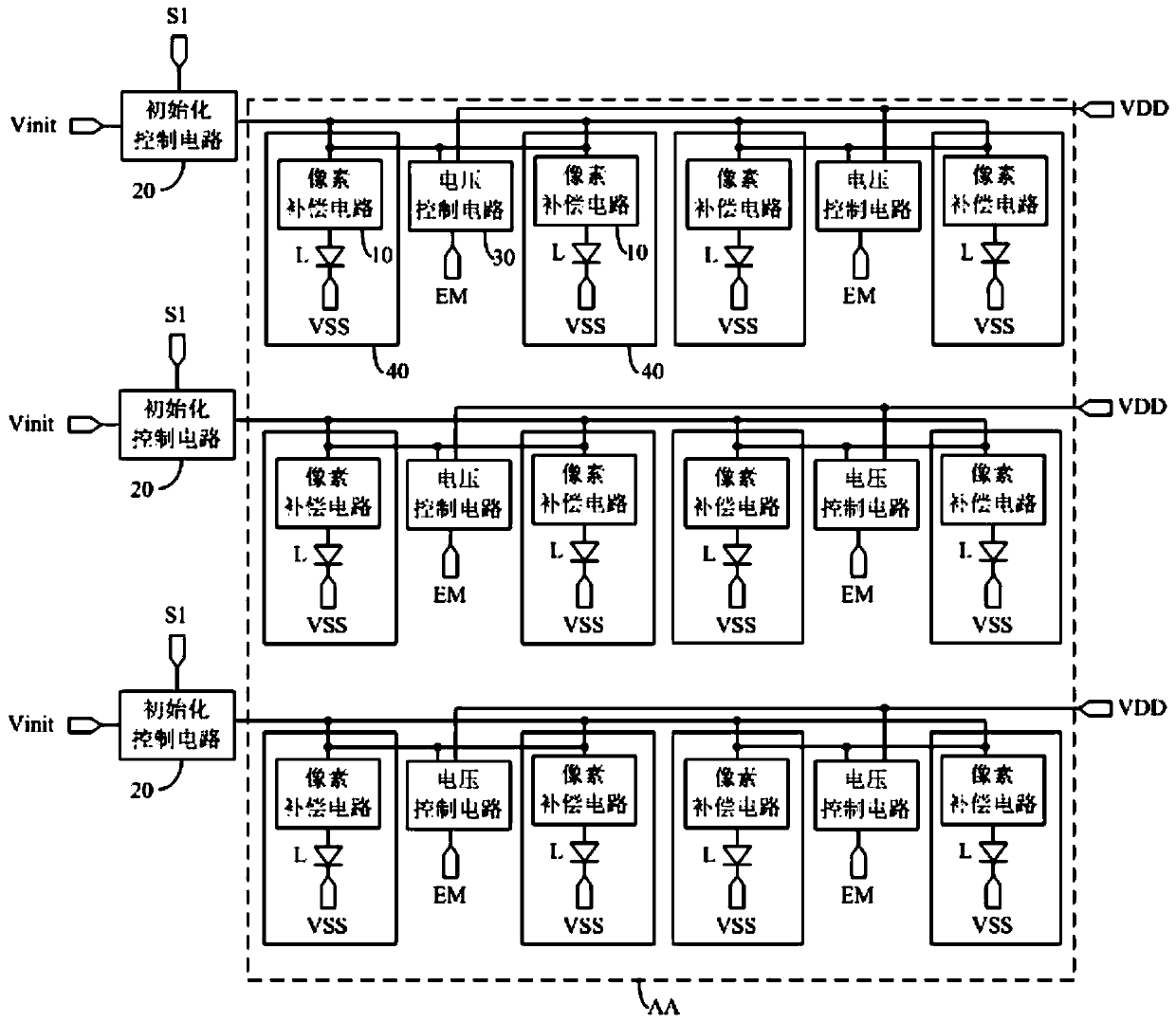
[0149] Figure 5c The pixel compensation circuits in all the pixel units 40 in the middle row share a voltage control circuit, that is, each pixel unit 40 includes 2 transistors and 2 capacitors respectively. Among them, only one row including two pixel units 40 is taken as an example, such as Figure 5c Shown, and with Figure 5c The structure of the circuit in the pixel unit 40 on the left and the pixel unit 40 on the right in the array substrate shown as an example is combined Figure 7a The timing diagram is shown for explanation. Specifically, select such as Figure 7a The shown input timing diagram has four stages: initialization stage T1, threshold compensation stage T2, data writing stage T3, and light-emitting stage T4. Among them, in the initialization phase T1 and the threshold compensation phase T2, the voltage of the signal output by the data signal terminal Data is V in , The V in Much smaller than the voltage V of the signal at the initialization signal terminal...


PUM


Abstract

The present invention discloses an array substrate, a driving method thereof, an organic light emitting display panel, and a display device. The array substrate comprises a plurality of light emitting devices, pixel compensation circuits connected to the light emitting devices, and a plurality of initialization control circuits located in a peripheral region of the array substrate. All of the pixel compensation circuits in each row share one initialization control circuit, which simplifies the structure of each pixel compensation circuit and reduces the occupation area of the pixel compensation circuits in the display area. The first pole of a driving transistor in each pixel compensation circuit is connected to the common initialization control circuit. The initialization control circuit is used to provide the signal of the initialization signal terminal to the first pole of each of the connected driving transistors under the control of the first scanning signal terminal, so that the first pole of the driving transistor can be prevented from being at the same bias voltage for a long time, the threshold voltage and mobility drift of the driving transistor can be improved to slow down the decay rate of the driving transistor, thereby improving the stability of the display.

Description

Technical field [0001] The present invention relates to the field of display technology, in particular to an array substrate, a driving method thereof, an organic light emitting display panel and a display device. Background technique [0002] Organic Light Emitting Diode (OLED) is one of the hotspots in the field of flat panel display research. Compared with Liquid Crystal Display (LCD), OLED display has low energy consumption, low production cost, self-luminous, and wide viewing angle. And the advantages of fast response. Currently, OLED displays have begun to replace traditional LCD displays in the display fields of mobile phones, tablet computers, and digital cameras. [0003] Unlike LCDs that use a stable voltage to control brightness, OLEDs are current driven and require a stable current to control their light emission. Generally, the OLED is driven to emit light by the driving transistor of the pixel driving circuit in the OLED display. Among them, when the driving transi...

Claims


Application Information

Patent Timeline
Patent Type & Authority Patents(China)
IPC IPC(8): G09G3/3208
CPCG09G3/3208
Inventor 向东旭李玥高娅娜陈泽源
Owner WUHAN TIANMA MICRO ELECTRONICS CO LTD
Why Eureka
Try Eureka