Low CTE glass with high UV-transmittance and solarization resistance

A technology of transmittance and ultraviolet rays, applied in the field of low CTE glass, can solve the problems of unsuitability, silicon substrate pollution, non-contamination, etc., and achieve the effect of long cycle life and good light fastness

Active Publication Date: 2017-08-29
SCHOTT GLASS TECH (SUZHOU) CO LTD
View PDF23 Cites 3 Cited by
  • Summary
  • Abstract
  • Description
  • Claims
  • Application Information

AI Technical Summary

Problems solved by technology

However, the borosilicate glasses disclosed in these documents are not suitable for use as carrier glass wafers for backgrinding and thinning of silicon for several reasons.
For example, one issue of US 5,547,904 A (Short AG) is that Li 2 O is used in borosilicate glass, which is not preferred in the semiconductor industry because the silicon substrate may be contaminated with lithium ions

Method used


Image

  • Low CTE glass with high UV-transmittance and solarization resistance
  • Low CTE glass with high UV-transmittance and solarization resistance
  • Low CTE glass with high UV-transmittance and solarization resistance

Examples


Embodiment Construction

[0050] The objects, features and advantages of the present invention will be shown in more detail by the examples and embodiments described hereinafter with reference to the accompanying drawings.

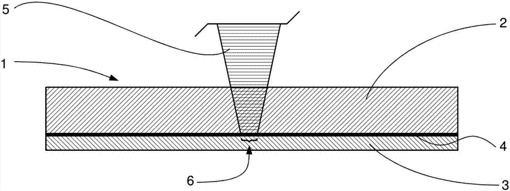
[0051] figure 1 A bonded product comprising a glass carrier wafer 2 during a debonding process by laser release is schematically shown. The bonded article 1 comprises a glass carrier wafer 2 made of glass according to the invention and a silicon substrate 3 bonded together by an adhesive layer 4 which can be deactivated by exposure to electromagnetic radiation. In this example, the adhesive layer 4 can be deactivated by UV radiation at a wavelength of 248 nm, so that the adhesion force is reduced or eliminated, so that the silicon substrate 3 can be debonded. The debonding (laser release) is achieved by irradiating the adhesive layer 4 with a laser 5 through the glass carrier wafer 2 . In a typical process, the wafer is mounted on a computer numerically controlled (CNC) controlle...


PUM

PropertyMeasurementUnit
transition temperatureaaaaaaaaaa
thicknessaaaaaaaaaa
thicknessaaaaaaaaaa

Abstract

A low CTE glass with a high UV-transmittance and high solarization resistance, a glass carrier wafer made of the low CTE glass and the use of such a glass carrier wafer. The glass comprises an alkaline metal oxide free composition of 50-75 mol%SiO2, 3-20 mol%Al2O3, 5-20 mol%B2O3, 0-15 mol%MgO, 0-15 mol%CaO, 0-15 mol%SrO, and 0-15 mol%BaO, where MgO+CaO+SrO+BaO amounts to 3 to 25 mol%and the average number of non-bridging oxygen per polyhedron (NBO) is equal or larger than -0.08 and equal or smaller than-0.38, or comprises an alkaline earth metal oxide free composition of 78-85 mol%SiO2, 0-7 mol%Al2O3, 8-15 mol%B2O3, 0-8 mol%Na2O, and 0-5 mol%K2O, where the NBO is equal or larger than -0.25 and equal or smaller than -0.10. The glass carrier wafer has a high UV-transmittance at a wavelength of 248 nm and/or 308 nm, good solarization resistance, a long recycling lifetime and reduced processing cost.

Description

technical field [0001] The present invention relates to a low CTE glass for glass carrier wafers having high UV transmittance and light fastness. The invention also relates to a glass carrier wafer made of said low CTE glass and its use as a carrier wafer in the processing of silicon substrates. Background technique [0002] Thinning of silicon substrates to meet the continuing demand for size reduction of, for example, integrated circuits has become a common process in the semiconductor industry. Silicon carrier wafers have been widely used as mechanical carriers for thinning and backgrinding of silicon substrates to facilitate handling of fragile thinned substrates. The silicon substrate is thus typically bonded to the carrier wafer by an adhesive. Depending on the adhesive, debonding of the silicon substrate from the carrier wafer after processing can be achieved, for example, by solvent release or thermal release. [0003] Glass has been used as a carrier wafer materi...

Claims


Application Information

Patent Timeline
Patent Type & Authority Applications(China)
IPC IPC(8): C03C3/091
CPCC03C3/091C03C4/0085
Inventor 薛军明平文亮范慧艳J·西默黑木浩
Owner SCHOTT GLASS TECH (SUZHOU) CO LTD
Why Eureka
Try Eureka