Polarization plate and image display device
A technology of image display device and polarizing plate, applied in optics, polarizing element, nonlinear optics, etc., to achieve the effect of effective blocking, excellent electromagnetic wave shielding, and excellent light transmittance
- Summary
- Abstract
- Description
- Claims
- Application Information
AI Technical Summary
Problems solved by technology
Method used
Image

Examples
Embodiment 1
[0114] Using a bar coater (manufactured by Daiichi Chemical Co., Ltd., product name "Barcoater No. 06"), the above-mentioned Metal nanowire dispersion liquid, and this coating film was dried at 100° C. for 2 minutes in a blower drier to form a conductive layer with a thickness of about 0.1 μm. In this way, a base material with a conductive layer formed of the base material and the conductive layer is produced. The total light transmittance of the substrate with the conductive layer was measured. The results are shown in Table 1.
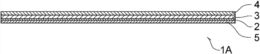
[0115] On the other hand, a polarizing film with a thickness of 190 μm (polyvinyl alcohol film dyed with iodine; manufactured by Nitto Denko Co., Ltd., trade name “NPF-SEG1425DU”) and a cellulose triacetate film with a thickness of 80 μm (manufactured by Fujifilm Corporation, trade name name "TD80UL"). The aforesaid polarizing film is bonded on the surface opposite to the surface on which the conductive layer is formed on the aforementioned base m...
Embodiment 2
[0118] Using a sputtering device equipped with a sintered compact target containing 90% by mass of indium oxide and 10% by mass of tin oxide, on one surface of a cycloolefin-based resin film (manufactured by Zeon Corporation, trade name "ZEONORZF16-100") with a thickness of 100 μm, An indium tin oxide film was formed and heat-treated at 130° C. for 90 minutes to form an ITO film (conductive layer) with a thickness of about 0.1 μm. Table 1 shows the measured values of the total light transmittance of the base material with the conductive layer.
[0119] In the same manner as in Example 1, a polarizing film and a cellulose triacetate film were bonded to the substrate with a conductive layer in Example 2, thereby producing a polarizing plate in Example 2.
[0120] Table 1 shows the surface resistance value and the measurement results of the shielding effect of the conductive layer of the polarizing plate.
Embodiment 3
[0122] Except that the bar coater was changed to "Barcoater No.08" manufactured by Daiichi Rika Co., Ltd., and the product name was "Barcoater No. 08", it was performed in the same manner as in Example 1 to form a conductive layer with a thickness of about 0.1 μm. After measuring the total light transmittance of the material, make a polarizing plate and measure its surface resistance and shielding effect. The results are shown in Table 1.
PUM
| Property | Measurement | Unit |
|---|---|---|
| Thickness | aaaaa | aaaaa |
| Thickness | aaaaa | aaaaa |
| Thickness | aaaaa | aaaaa |
Abstract
Description
Claims
Application Information
 - R&D
- Intellectual Property
- Life Sciences
- Materials
- Tech Scout
- Unparalleled Data Quality
- Higher Quality Content
- 60% Fewer Hallucinations
Browse by: Latest US Patents, China's latest patents, Technical Efficacy Thesaurus, Application Domain, Technology Topic, Popular Technical Reports.
© 2025 PatSnap. All rights reserved.Legal|Privacy policy|Modern Slavery Act Transparency Statement|Sitemap|About US| Contact US: help@patsnap.com