Micro-fluidic chip and manufacturing method thereof

A technology of microfluidic chips and manufacturing methods, applied in chemical instruments and methods, measuring devices, instruments, etc., can solve the problems of increasing purity, decreasing adsorption efficiency, shortening the time of adsorption reaction, etc., to avoid damage to cell activity, Reduce the separation and adsorption speed and avoid the effect of cell loss

Active Publication Date: 2017-09-01
SUZHOU INST OF NANO TECH & NANO BIONICS CHINESE ACEDEMY OF SCI
View PDF5 Cites 7 Cited by
  • Summary
  • Abstract
  • Description
  • Claims
  • Application Information

AI Technical Summary

Problems solved by technology

[0009] 1. In the immunomagnetic bead method, the separation and capture process is complicated, and the separation cost is high; and the sample volume used in batch processing is large, and the separation efficiency is low
In addition, the immunomagnetic bead method requires pretreatment of the cells, which inevitably causes cell loss during the transfer process, which may affect the detection results for rare cells
Furthermore, in the immunomagnetic bead method, although fluorescent dyes are used to distinguish different cells, due to serious cell contamination, it is unfavorable for cell identification, technology and cell analysis.
[0010] 2. The existing microfluidic technology that only uses physical methods to separate cells has no obvious difference in physical characteristics such as size and deformation, and even some characteristic areas overlap. The purity of separation is often low, and further capture of cells is still requi

Method used


Image

  • Micro-fluidic chip and manufacturing method thereof
  • Micro-fluidic chip and manufacturing method thereof
  • Micro-fluidic chip and manufacturing method thereof

Examples


Embodiment Construction

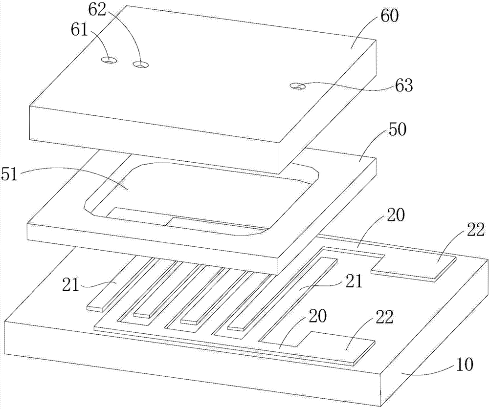
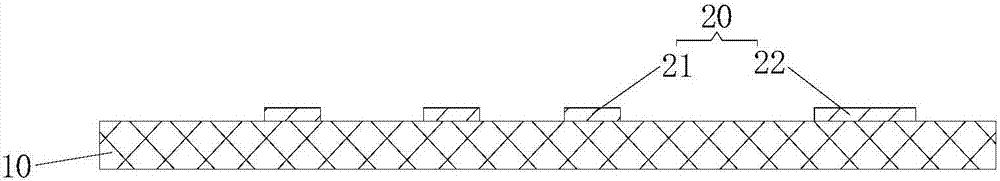
[0037] Hereinafter, embodiments of the present invention will be described in detail with reference to the accompanying drawings. This invention may, however, be embodied in many different forms and should not be construed as limited to the specific embodiments set forth herein. Rather, the embodiments are provided to explain the principles of the invention and its practical application, thereby enabling others skilled in the art to understand the invention for various embodiments and with various modifications as are suited to particular intended uses.

[0038] First, a necessary explanation of the nouns that will be used in the following descriptions:

[0039] Dielectrophoresis (DEP): A phenomenon in which neutral particles are polarized and move under the action of a non-uniform electric field. The size of the dielectrophoretic force is related to the size of the object, the electrical properties, the electrical properties of the surrounding medium, and the field strength ...


PUM


Abstract

The invention provides a micro-fluidic chip, which includes: a substrate; shaping electrode on a substrate; a gear shaping electrode on the substrate; an insulating layer covering the gear shaping electrode on the substrate; an electrode slice in the insulating layer and in electrical contact with the gear shaping electrode; a patterned bonding member with a hollow structure on the insulating layer; and a cover plate for sealing the hollow structure of the patterned bonding member therein, wherein the cover plate has an inlet hole and an outlet hole that are both communicated with the hollow structure. The invention also provides a manufacturing method of the micro-fluidic chip. The invention combines immune adsorption with the electrical characteristics of cells, a non-uniform electric field can be formed in a flow channel through the gear shaping electrode structure simply, cells receive a dielectrophoresis force, and non-targeted cells can break away without affecting targeted cell adsorption, thus maintaining high efficiency of cell immune adsorption while improving the adsorption purity under a flow rate conducive to specific adsorption.

Description

technical field [0001] The invention belongs to the technical field of semiconductor processing, and in particular relates to a microfluidic chip and a manufacturing method thereof. Background technique [0002] Circulating tumor cells (CTCs), as an important marker of cancer metastasis, are tumor cells that are generated from the lesion in the early stage of cancer and spread to other organs through the peripheral blood. Sensitive detection of CTCs from peripheral blood cells is of great significance for the diagnosis and prevention of early tumors. High-purity, high-efficiency capture and effective analysis of CTCs is expected to further understand the formation mechanism of tumors and prevent the occurrence of lesions from the root. However, due to the rarity of circulating tumor cells (1 / 10 7 ), a large number of impurity cells will surely become an obstacle in its efficient and high-purity separation and capture process, how to obtain target cells (ie circulating tumo...

Claims


Application Information

Patent Timeline
IPC IPC(8): B01L3/00G01N27/447
CPCB01L3/5027B01L3/502707B01L2200/10G01N27/44791
Inventor 王慧沈文江
Owner SUZHOU INST OF NANO TECH & NANO BIONICS CHINESE ACEDEMY OF SCI
Why Eureka
Try Eureka