
Architecture and design method of fpga BRAM based on non-volatile memory

A non-volatile, architecture design technology, applied in CAD circuit design, instrumentation, calculation, etc., can solve the problems of delay and high power consumption

Active Publication Date: 2019-08-30
SHANDONG UNIV
View PDF7 Cites 0 Cited by
  • Summary
  • Abstract
  • Description
  • Claims
  • Application Information

AI Technical Summary

Problems solved by technology

Although MLC technology greatly improves the storage density, because it takes two steps to read and write data in MLC STT-MRAM, the delay and power consumption of reading data from MLC or designing hard-bit is obviously higher than that of soft-bit

Method used

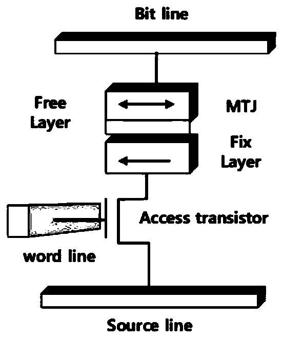
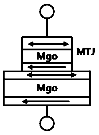

Image

  • Architecture and design method of fpga BRAM based on non-volatile memory
  • Architecture and design method of fpga BRAM based on non-volatile memory
  • Architecture and design method of fpga BRAM based on non-volatile memory

Examples


Embodiment approach

[0089] like Figure 5 As shown, the process of using VTR7.0 for FPGA design is:

[0090] Step (1): Input the detailed description of the circuit and architecture. The benchmark requires the use of Verilog 1995 version. The detailed description of the architecture refers to the description of the underlying hardware by k6_frac_N10_mem32K_40nm.xml;

[0091] Step (2): Carry out logic synthesis and optimization;

[0092] Perform logic synthesis on the input RTL level circuit to generate a gate level circuit (generate .blif file). During the optimization process, remove some useless redundant wiring mappings in the circuit.

[0093] Step (3): Packing, packing gate-level circuits into logic blocks, and generating netlist file .net;

[0094] Step (4): carry out the layout, which means that the tool automatically arranges the optimal position of each logic block;

[0095] Step (5): Perform wiring. Wiring means that the tool automatically connects each logic block, after which the c...


PUM


Abstract

The invention provides a nonvolatile memory-based FPGA BRAM architecture and a design method. The method comprises the steps of inputting a benchmark circuit and an architecture detail description; compiling the benchmark circuit into an RTL level circuit, performing logic synthesis on the RTL level circuit to generate a gate level circuit, and in a process of optimizing the gate level circuit, removing mapping of redundant connection wires in the RTL level circuit; performing packaging: packaging the optimized gate level circuit into logic blocks; performing optimal position arrangement on the generated logic blocks by utilizing an SA algorithm based on a tool VTR7.0; performing wiring: performing wiring on the generated logic blocks based on the tool VTR7.0, and after the logic blocks are subjected to the wiring, obtaining key path delays and bus lengths of the benchmark circuit; and performing performance assessment on the key path delays and the bus lengths, and outputting a minimum key path delay and a shortest bus length.

Description

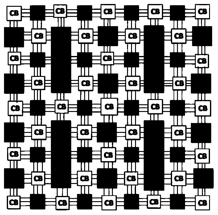
technical field [0001] The invention relates to an FPGA BRAM architecture and a design method based on a nonvolatile memory. Background technique [0002] In the era of heterogeneous computing, from embedded devices to high-performance computing platforms, FPGA has become the choice favored by developers. The architecture also follows Moore's Law to provide more on-chip resources. However, the exponential increase in computing energy consumption (including video processing and machine learning algorithms, etc.) also brings more memory wall problems for FPGAs to implement memory-intensive functions. [0003] figure 1 It shows the traditional architecture of FPGA, where logic configuration modules CLB (configurable logic blocks), connection boxes CB (connecting boxes), switch boxes SB (switch boxes) and BRAM (blockRAMs) are distributed in the architecture, where BRAM is a configurable memory module , allowing fast data storage. In the past few generations of high-end Xilinx...

Claims


Application Information

Patent Timeline
Patent Type & Authority Patents(China)
IPC IPC(8): G06F17/50
CPCG06F30/39
Inventor 鞠雷李涵涵贾智平隋晓金赵梦莹
Owner SHANDONG UNIV
Learn More