Array substrate and preparation method therefor, and display apparatus

An array substrate, extending direction technology, used in semiconductor/solid-state device manufacturing, optics, instruments, etc., can solve problems such as data line disconnection

Active Publication Date: 2017-10-03
BOE TECH GRP CO LTD
View PDF4 Cites 13 Cited by
  • Summary
  • Abstract
  • Description
  • Claims
  • Application Information

AI Technical Summary

Problems solved by technology

When coating the photoresist (the photoresist is on the surface of the top molybdenum-niobium layer) on the surface of the conductive film layer composed of the bottom molybdenum-niobium layer, copper metal layer and top molybdenum-niobium layer, due to the difference between the photoresist and the top molybdenum-niobium layer The adhesion is low, so the photoresist is easy to produce gaps at the above-mentioned climbing places. In the subsequent etching process, the etching solution invades the conductive film layer from the above-mentioned gaps, which easily causes the formed data lines to break.

Method used


Image

  • Array substrate and preparation method therefor, and display apparatus
  • Array substrate and preparation method therefor, and display apparatus
  • Array substrate and preparation method therefor, and display apparatus

Examples


Embodiment Construction

[0029] The following will clearly and completely describe the technical solutions in the embodiments of the present invention with reference to the accompanying drawings in the embodiments of the present invention. Obviously, the described embodiments are only some, not all, embodiments of the present invention. Based on the embodiments of the present invention, all other embodiments obtained by persons of ordinary skill in the art without making creative efforts belong to the protection scope of the present invention.

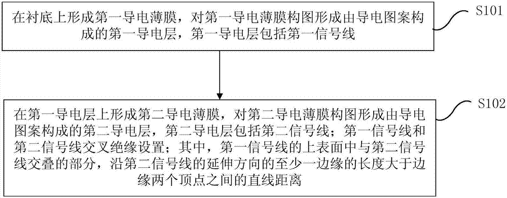
[0030] An embodiment of the present invention provides a method for preparing an array substrate, such as figure 1 shown, including:

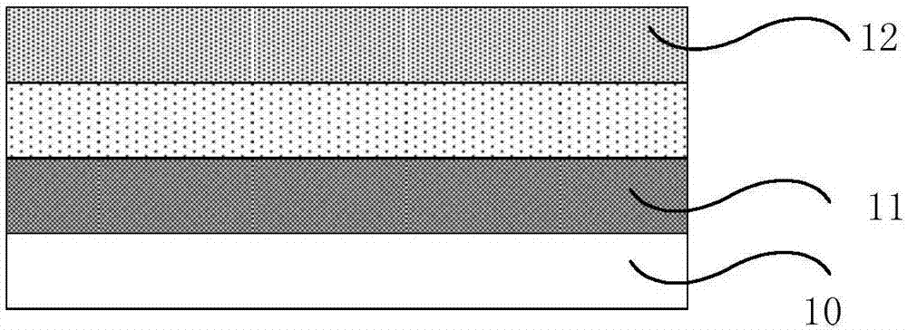
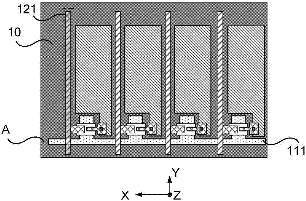
[0031] Step S101, such as figure 2 As shown, a first conductive film is formed on a substrate 10, and the first conductive film is patterned to form a first conductive layer 11 made of conductive patterns, as image 3 As shown, the first conductive layer 11 includes a first signal line 111 .

[0032] It should be noted that...


PUM


Abstract

Embodiments of the invention provide an array substrate and a preparation method therefor, and a display apparatus, relate to the technical field of display, and aim to lower line-breaking probability of signal lines on the top layer in climbing when the crossed signal lines are formed in the array substrate. The preparation method comprises the steps of forming a first conductive thin film on a substrate, performing graphic composition on the first conductive thin film to form a first conductive layer formed by conductive patterns, wherein the first conductive layer comprises a first signal line; forming a second conductive thin film on the first conductive layer, performing graphic composition on the second conductive thin film to form a second conductive layer formed by conductive patterns, wherein the second conductive layer comprises a second signal line; and performing crossing insulation treatment on the first signal line and the second signal line, wherein the length of at least one edge is greater than the linear distance between two top points of the edge in the extension direction of the second signal line on the part, overlapped with the second signal line, of the upper surface of the first signal line.

Description

technical field [0001] The present invention relates to the field of display technology, in particular to an array substrate, a preparation method thereof, and a display device. Background technique [0002] When preparing the array substrate, copper is usually used as the material of the source-drain metal layer including the source electrode, the drain electrode and the data line in the array substrate. Due to the active nature of copper, it is easy to diffuse into other film layers, and under the action of high temperature or external electric field, copper is easy to be oxidized, which affects the display effect of the display device formed by the array substrate. Therefore, the material usually constituting the source-drain metal layer also includes molybdenum-niobium (chemical formula: MoNb), and the molybdenum-niobium layer is usually formed on the upper and lower surfaces of the copper metal layer to protect the copper. [0003] However, the adhesion of photoresist ...

Claims


Application Information

Patent Timeline
IPC IPC(8): H01L21/77H01L27/12
CPCH01L27/1244H01L27/1259G02F1/136286G02F1/13629G02F1/136295
Inventor 黎午升
Owner BOE TECH GRP CO LTD
Why Eureka
Try Eureka