Method and device for machining wafer by using laser

A laser processing and wafer technology, used in metal processing equipment, laser welding equipment, manufacturing tools, etc., can solve the problems of inability to remove clean edges, damage devices, etc., achieve high uniformity, uniform grooves, and improve yield. Effect

Active Publication Date: 2017-10-17
北京中科镭特电子有限公司
View PDF4 Cites 1 Cited by
  • Summary
  • Abstract
  • Description
  • Claims
  • Application Information

AI Technical Summary

Problems solved by technology

[0004] However, the existing laser cutting is to form a groove on the wafer. Since the laser is Gaussian distributed during cutting, the shape of the groove is "V" and the edge cannot be removed cleanly.
So when cutting with a blade after etching, the cutting may damage the device

Method used


Image

  • Method and device for machining wafer by using laser
  • Method and device for machining wafer by using laser
  • Method and device for machining wafer by using laser

Examples


Embodiment Construction

[0046]In order to make the purpose, technical solutions and advantages of the embodiments of the present invention clearer, the technical solutions in the embodiments of the present invention will be clearly and completely described below in conjunction with the drawings in the embodiments of the present invention. Obviously, the described embodiments It is only some embodiments of the present invention, but not all embodiments. Based on the embodiments of the present invention, all other embodiments obtained by persons of ordinary skill in the art without making creative efforts belong to the protection scope of the present invention.

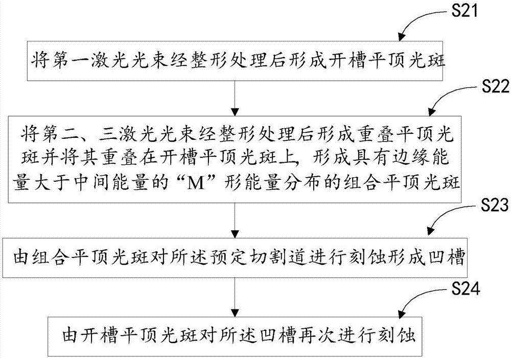
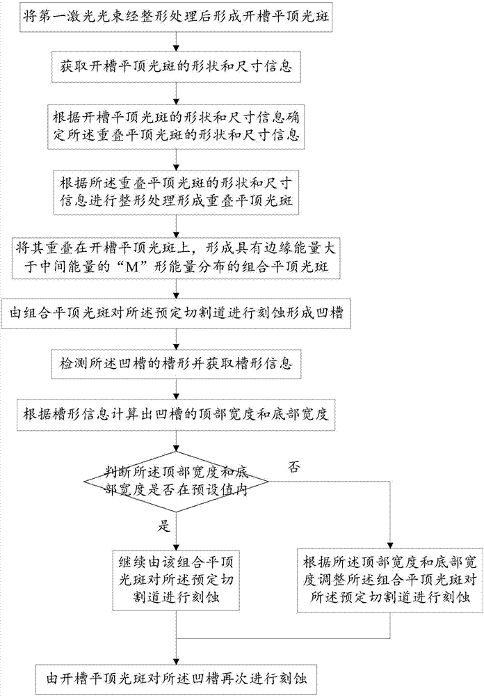
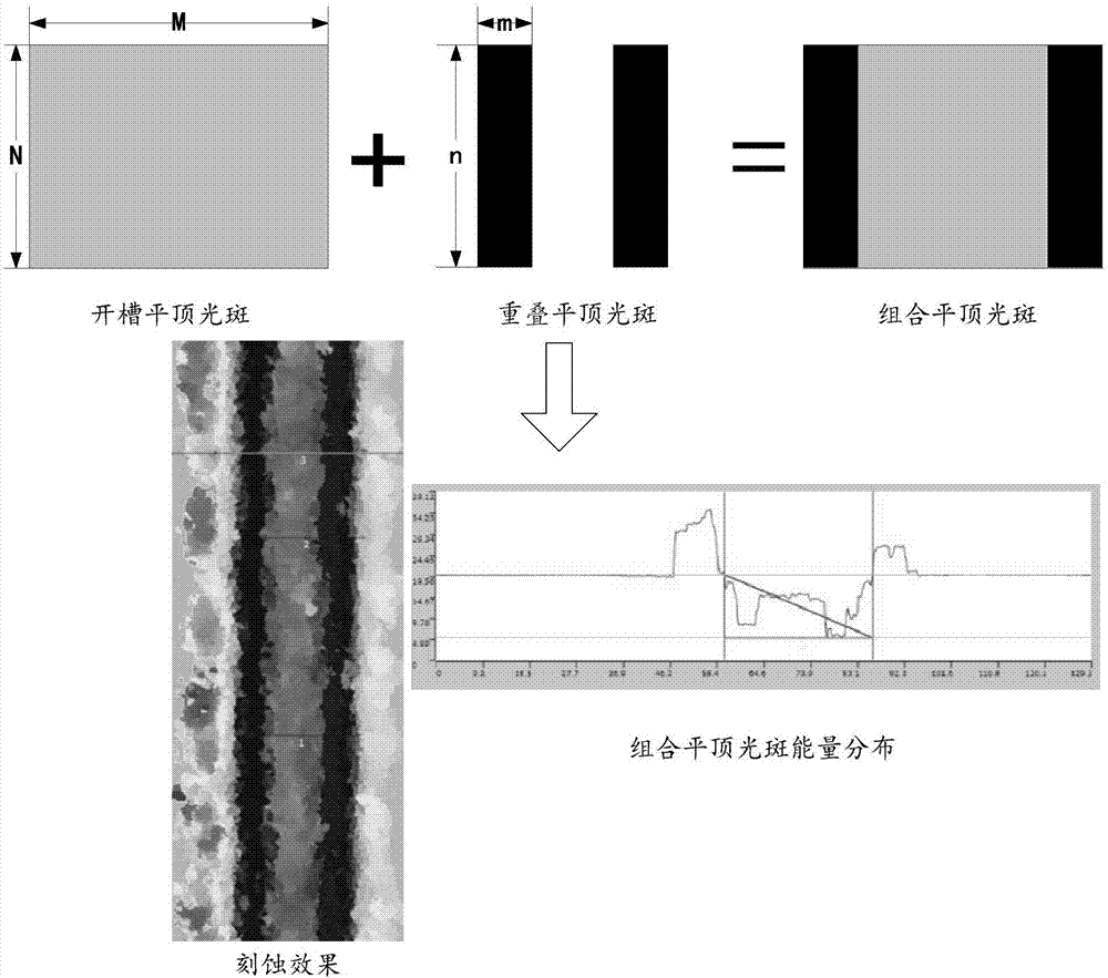
[0047] Embodiments of the present invention provide a method for laser processing wafers, such as figure 1 As shown, changing the relative position between the laser beam and the predetermined cutting line along the direction of the predetermined cutting line on the upper surface of the wafer to form a groove on the predetermined cutting line,...


PUM


Abstract

The invention provides a method and device for machining a wafer by using laser. According to the method, by changing the relative position between a laser beam and a predetermined grooving way in the direction of the predetermined grooving way on the upper surface of the wafer, a groove is formed in the predetermined grooving way; and the method comprises the steps that a first laser beam forms a grooving flat-topped light spot after being subjected to shaping treatment; a second laser beam and a third laser beam form overlapping flat-topped light spots after being subjected to shaping treatment, the grooving flat-topped light spot is overlapped by the overlapping flat-topped light spots to form a combined flat-topped light spot, wherein energy distribution of the combined flat-topped light spot is in an M shape, namely, the edge energy of the combined flat-topped light spot is greater than the middle energy of the combined flat-topped light spot; sculpturing is conducted on the predetermined grooving way through the combined flat-topped light spot to form the groove; and sculpturing is conducted on the groove again through the grooving flat-topped light spot. By adopting the method and device for machining the wafer by using the laser, the two sides of the edge of the grooving flat-topped light spot are overlapped by the overlapping flat-topped light spots correspondingly to form the combined flat-topped light spot with the M-shaped energy distribution, namely the edge energy is greater than the middle energy, so that the accuracy of the groove-shaped structure of the groove and the yield of wafer machining can be enhanced.

Description

technical field [0001] The invention relates to the technical field of semiconductor processing, in particular to a method and device for laser processing wafers. Background technique [0002] In recent years, with the continuous reduction of the feature size of semiconductor devices and the continuous improvement of chip integration, the parasitic capacitance between metal interconnections and multilayer wiring and the resistance of metal wires have increased sharply, resulting in RC delays, A series of problems such as increased power consumption limit the development of high-speed electronic components. When the feature size of the device is smaller than 90nm, the wafer must use low dielectric constant material instead of traditional SiO 2 Layer (K ​​= 3.9 ~ 4.2), commonly used Low-K materials include Dow Corning's FOx and porous SiLK materials, Applied Materials' black diamond series low-K thin film materials, Novellus System's CORAL, Intel's CDO and NEC's FCN+ organic...

Claims


Application Information

Patent Timeline
Patent Type & Authority Applications(China)
IPC IPC(8): B23K26/362B23K26/073B23K26/03B23K26/70
CPCB23K26/032B23K26/073B23K26/361B23K26/702
Inventor 刘嵩侯煜张紫辰
Owner 北京中科镭特电子有限公司
Why Eureka
Try Eureka