Method of manufacturing touch control display device

A manufacturing method and touch display technology, applied in semiconductor/solid-state device manufacturing, data processing input/output process, optics, etc., can solve problems such as product yield and manufacturing cost increase, and achieve good sensing performance, good Carrier mobility, effects of good photosensitivity

Active Publication Date: 2017-10-20
AU OPTRONICS CORP
View PDF7 Cites 6 Cited by
  • Summary
  • Abstract
  • Description
  • Claims
  • Application Information

AI Technical Summary

Problems solved by technology

[0002] At present, on-cell display touch technology requires setting touch elements outside the display for touch sensing operation, so as the screen size gradually enlarges, it will face the shortcomings of product yield and manufacturing cost.

Method used


Image

  • Method of manufacturing touch control display device
  • Method of manufacturing touch control display device
  • Method of manufacturing touch control display device

Examples


Embodiment Construction

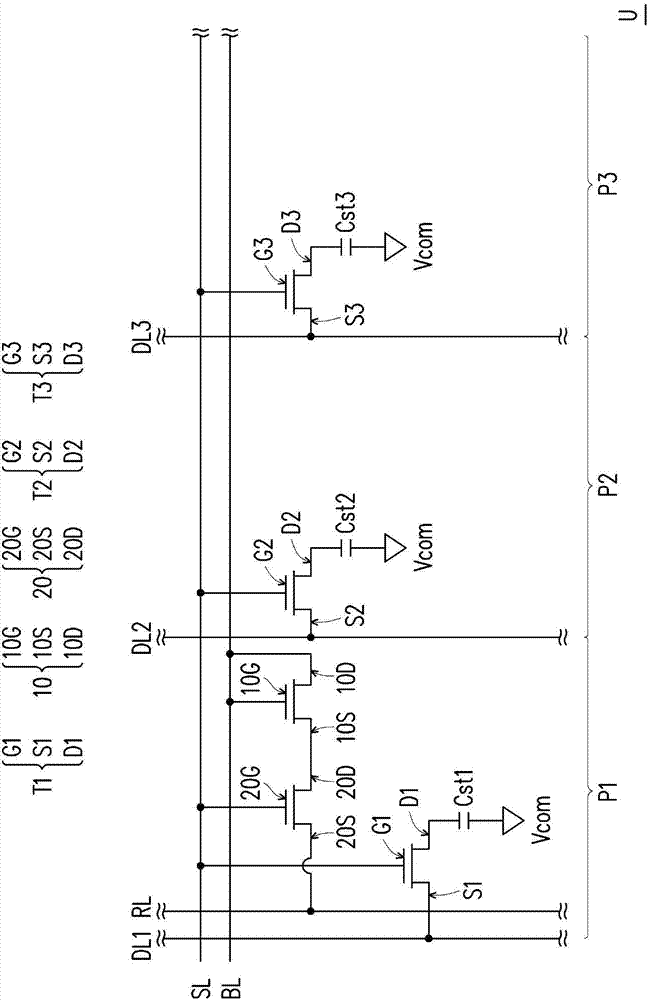
[0076] The touch display device of the present invention can be, for example, a touch liquid crystal display device. Anyone skilled in the art should understand that a touch liquid crystal display device generally includes a pixel array formed by a plurality of identical or similar pixel unit arrays. For clarity, figure 1 Only one pixel unit U is shown in .

[0077] figure 1It is a partial equivalent circuit diagram of a touch display device according to an embodiment of the present invention. Please refer to figure 1 The pixel unit U of the touch display device includes scan lines SL, data lines DL1˜DL3, sensing signal lines BL, readout lines RL, sub-pixel units P1, sub-pixel units P2, and sub-pixel units P3.

[0078] In this embodiment, the sub-pixel unit P1 includes the active element T1, the sensing element 10, the switching element 20, and the capacitor Cst1; the sub-pixel unit P2 includes the active element T2 and the capacitor Cst2; the sub-pixel unit P3 includes th...


PUM


Abstract

A method of manufacturing a touch control display device includes the following steps: forming a sensing element on a substrate, and forming a sensing signal line electrically connected with the sensing element; the step of forming the sensing element includes: forming a semiconductor layer on the substrate, the semiconductor layer including a semiconductor pattern of the sensing element; forming a gate insulating layer on the semiconductor layer; forming a first conductor layer on the gate insulating layer; forming an interlaye insulating layer on the gate insulating layer; performing a tempering process; after the tempering process, removing the interlayer insulating layer in a gate predetermined region; removing the first conductor layer in the gate predetermined region; forming a gate in the gate predetermined region; and forming a second conductor layer, wherein the second conductor layer includes a source electrode and a drain electrode of the sensing element that are electrically connected with the semiconductor pattern of the sensing element.

Description

technical field [0001] The present invention relates to a manufacturing method of a display device, and in particular to a manufacturing method of a touch display device. Background technique [0002] At present, the on-cell display touch technology requires setting touch elements outside the display for touch sensing operation, so as the screen size gradually enlarges, it will face the disadvantages of greatly increasing product yield and manufacturing cost. The embedded (In-cell) optical touch technology can be multi-touch and directly embed the touch sensing element on the array substrate of the liquid crystal display (Liquid Crystal Display, LCD), so that the use of existing production capacity, adjustment The photomask process can be produced without additional investment in huge capital expenditures, so it can reduce the cost of lamination and assembly, and reduce the thickness and weight of the device. It has the advantages of high yield, low cost, and no size limit. ...

Claims


Application Information

Patent Timeline
Patent Type & Authority Applications(China)
IPC IPC(8): G06F3/041H01L27/12H01L21/77
CPCG06F3/041H01L27/1214H01L27/1259G06F2203/04103G06F2203/0338H01L27/1255G06F3/0412G06F3/042H01L29/4908H01L29/78633G02F1/13685G02F1/133357G02F1/133345G02F1/13338G02F1/136209G02F1/136213G02F1/136227G02F1/136286G02F1/1368G02F2201/121G02F2201/123G02F2202/104H01L27/127
Inventor 陈信学陈亦伟
Owner AU OPTRONICS CORP
Why Eureka
Try Eureka