Semiconductor packaging method capable of improving precision of upper cover plate

A packaging method and semiconductor technology, which is applied in the direction of semiconductor devices, semiconductor/solid-state device manufacturing, semiconductor/solid-state device components, etc., to achieve the effect of improving assembly yield

Inactive Publication Date: 2017-10-20
POWERTECH TECHNOLOGY +1
View PDF4 Cites 2 Cited by
  • Summary
  • Abstract
  • Description
  • Claims
  • Application Information

AI Technical Summary

Problems solved by technology

Since the final packaging product requires the outer surface of the transparent material cover to be clean and flawless without leaving any imprints or marks, there is no way to correctly identify where the transparent material cover is installed when using an automatic machine to assemble the transparent cover. The position on the chip, after the assembly is completed, the position error of the transparent material cover will be greater than + / -50 microns (µm)

Method used


Image

  • Semiconductor packaging method capable of improving precision of upper cover plate
  • Semiconductor packaging method capable of improving precision of upper cover plate
  • Semiconductor packaging method capable of improving precision of upper cover plate

Examples


Embodiment Construction

[0036] The present invention will be further described below in conjunction with the accompanying drawings and specific embodiments, so that those skilled in the art can better understand the present invention and implement it, but the examples given are not intended to limit the present invention.

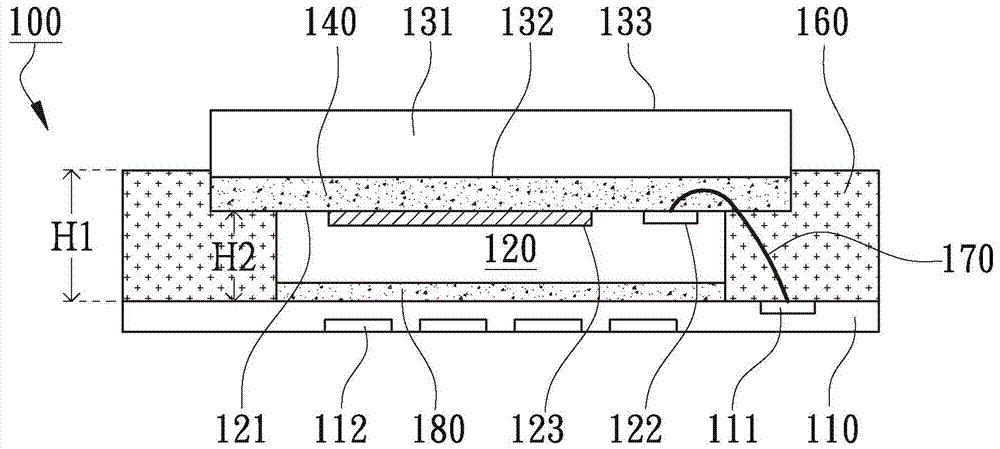
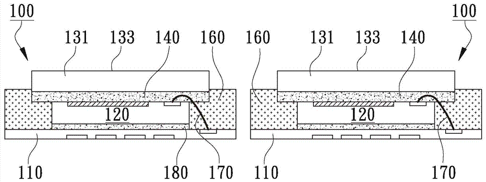
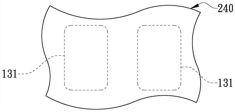
[0037] According to a specific embodiment of the present invention, a semiconductor packaging structure 100 manufactured by a semiconductor packaging method is illustrated in figure 1 cross-sectional schematic diagram. Figure 2A to Figure 2I A schematic cross-sectional view of components showing each main step in a semiconductor packaging method. Figure 3A to Figure 3D A schematic diagram of the surface of the cover plate is shown in the process of adding identification feature points in the semiconductor packaging method.

[0038] see figure 1 , a semiconductor packaging structure 100 disclosed in the present invention mainly includes a substrate 110 , a chip 120 , a cover pl...


PUM


Abstract

The invention discloses a semiconductor packaging method capable of improving the precision of an upper cover plate. A plurality of chips are arranged on a substrate, the active sides of the chips are arranged far from the substrate and electrically connected to the substrate. Before transparent cover plates are assembled to the active sides of the chips, an identification characteristic point layer is added to the external surface of each cover plate to facilitate identification and position calibration by an assembly machine to held the assembly machine to calibrate position. The cover plates are assembled afterwards. The assembly qualified rate is greatly improved. After the upper covers are assembled, the characteristic points on the surfaces of the cover plates are removed. Die sealing and single-body cutting and subsequent packaging processes are than conducted. The position error of assembled cover plates after assembly can be reduced, and the surfaces of the cover plates are smooth, clean and free of stain and marks.

Description

technical field [0001] The invention relates to the field of induction chip packaging, in particular to a semiconductor packaging method for improving the precision of an upper cover plate. Background technique [0002] In general, chip packaging products mainly use epoxy resin to mold and coat the chip on a substrate, and then perform singulation to complete the package. One of the chip packaging products is required to be equipped with a cover on the exterior surface. For example, a fingerprint sensor chip should be equipped with a transparent material cover on the package surface, and a high-heat chip should be equipped with a high thermal conductivity metal cover on the package surface. A packaging method for the top cover directly uses a large-area cover mother chip when molding, and cuts the cover master chip in addition to the encapsulant and the substrate when cutting the order. The cutting stress will remain between the cover plate and the chip, or cause cracks bet...

Claims


Application Information

Patent Timeline
Patent Type & Authority Applications(China)
IPC IPC(8): H01L21/56H01L23/544
CPCH01L23/544H01L21/561H01L2224/8592H01L2224/97H01L2224/48091H01L2224/73265H01L2924/00014
Inventor 苗红燕华毅刘志凌
Owner POWERTECH TECHNOLOGY
Why Eureka
Try Eureka