QFN chip

A chip and chip body technology, applied in electrical components, electrical solid devices, circuits, etc., can solve problems such as poor welding, small contact area, and substandard coverage, and achieve the effect of improving bonding force and increasing contact area.

Active Publication Date: 2017-10-20
ZHENGZHOU YUNHAI INFORMATION TECH CO LTD
View PDF7 Cites 10 Cited by
  • Summary
  • Abstract
  • Description
  • Claims
  • Application Information

AI Technical Summary

Problems solved by technology

However, in the production process, since the surfaces of the two pads to be welded are a plane with a large cross-sectional area, the coverage area of ​​the solder paste on the two pads is not up to standard during soldering, resulting in a small contact area between the two pads (The contact between the two pads is realized by solder paste), resulting in poor soldering, which greatly affects the soldering quality and product quality

Method used


Image

  • QFN chip
  • QFN chip
  • QFN chip

Examples


Embodiment 1

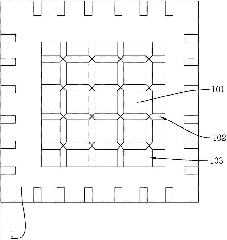
[0029] Such as figure 1 Shown, a kind of QFN chip comprises chip body 1, and this chip body 1 is provided with pad 101, and this pad 101 is provided with a plurality of transverse tin-conducting grooves 102 and a plurality of vertical tin-conducting grooves 103, and the The transverse tin-conducting grooves 102 and the longitudinal tin-conducting grooves 103 are arranged to cross each other and communicate with each other.

[0030] Preferably, all the transverse tin-conducting grooves 102 and all the longitudinal tin-conducting grooves 103 are arranged perpendicular to each other; The pads 101 are arranged in an array along the length direction.

[0031] The distance between two adjacent horizontal tin-conducting grooves 102 is equal to the distance between two adjacent vertical tin-conducting grooves 103 , and the width of the transverse tin-conducting grooves 102 is the same as the width of the longitudinal tin-conducting grooves 103 .

Embodiment 2

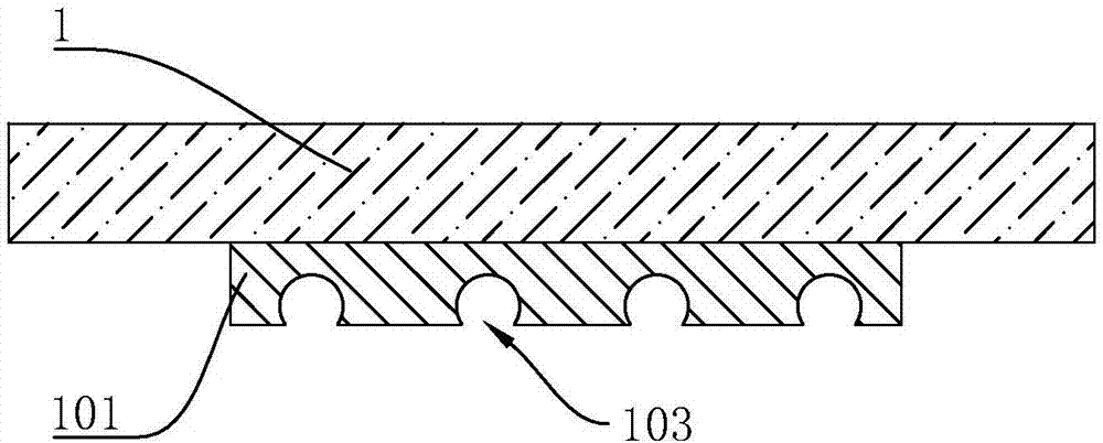
[0033] The structure of this embodiment is basically the same as that of Embodiment 1, the difference being that both the transverse tin-conducting groove 102 and the longitudinal tin-conducting groove 103 are omega grooves (see figure 2 ).

Embodiment 3

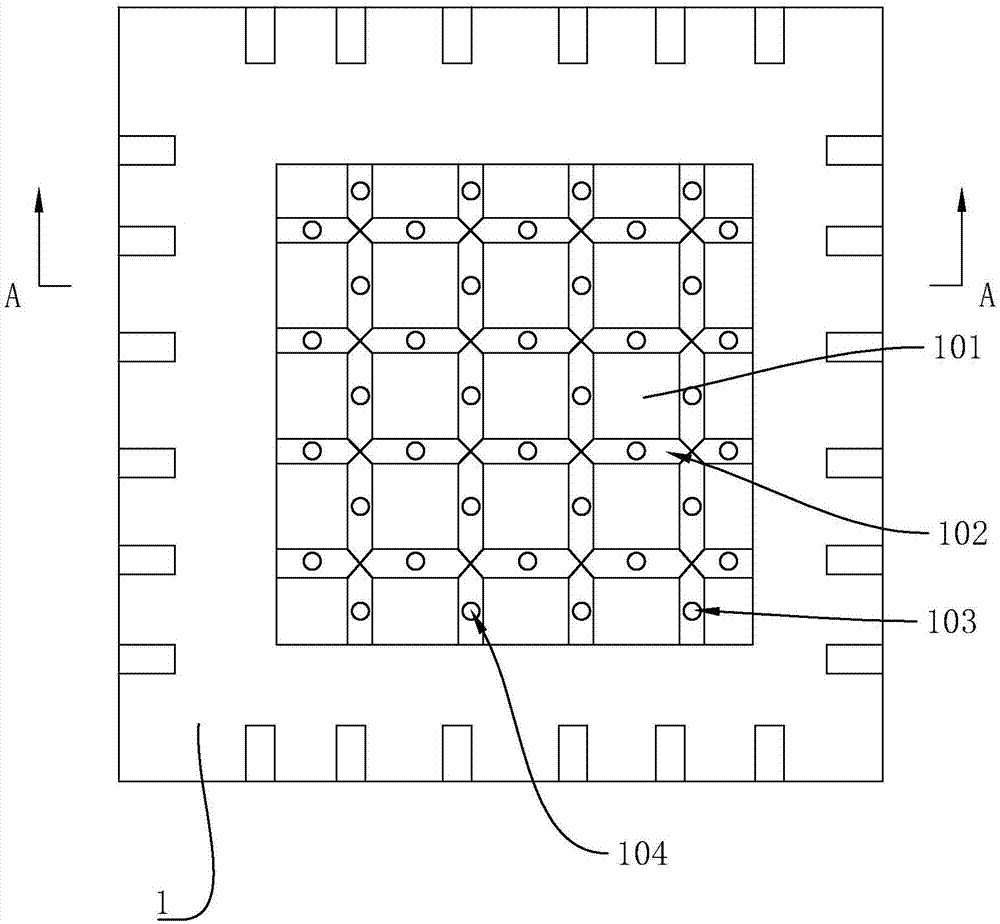
[0035] The structure of this embodiment is basically the same as that of Embodiment 1, the difference is that at least one concave hole 104 is provided on the pad 101 corresponding to the horizontal tin-conducting groove 102 and the vertical tin-conducting groove 103, and the concave hole 104 is along the The height direction of the pad 101 extends, and the concave hole 104 communicates with the transverse tin-conducting groove 102 or the longitudinal tin-conducting groove 103 (see image 3 and Figure 4 ). In this scheme, each concave hole 104 located in the horizontal tin-conducting groove 102 and the longitudinal tin-conducting groove 103 corresponds to a small pad (the small pad is formed by the horizontal tin-conducting groove 102 and the vertical tin-conducting groove 102). The groove 103 divides the pad 101).


PUM


Abstract

The invention discloses a QFN chip comprising a chip body which is provided with a welding pad. The welding pad is provided with multiple transverse tin guide grooves and multiple longitudinal tin guide grooves. The transverse tin guide grooves and the longitudinal tin guide grooves are arranged in a mutual intersection way and mutually communicated. Firstly tin paste is brushed on the welding pad of a circuit board, then the chip body is moved to the circuit board and the welding pad on the chip body and the welding pad on the are adhered together through the tin paste, and then heating is performed and the tin paste is molten and welding can be realized. The welding pad is segmented into multiple small blocks by the transverse tin guide grooves and the longitudinal tin guide grooves in the process so that flowing of the tin paste after heating is facilitated and the cover area of the tin paste on the two welding pads can be increased; meanwhile, the flowing paths can be provided for the tin paste by the transverse tin guide grooves and the longitudinal tin guide grooves so that the welding area and the coverage rate of the tin paste on the two welding pads can be increased, the welding strength can be increased and the welding quality and the product quality can also be effectively enhanced.

Description

technical field [0001] The invention relates to the technical field of QFN packaging, in particular to a QFN chip. Background technique [0002] At present, the integration degree of electronic parts is getting higher and higher, and more and more electronic parts are designed with IC (integrated circuit integrated circuit) with higher integration degree. Usually in the server system or personal computer, it is a motherboard design, and the number of ICs with a high degree of integration is very large. However, due to the limited space on the motherboard, the risk of ESD (Electro-Static discharge) is also relatively high, and the packaging method using pins (pins) is gradually eliminated. [0003] At this stage, the most commonly used package is QFN package (Quad Flat No-lead Package). The specific method of QFN package is: there are pads (copper foil) on both the circuit board and the QFN chip, and two pads Soldered together to achieve a QFN package. However, in the prod...

Claims


Application Information

Patent Timeline
Patent Type & Authority Applications(China)
IPC IPC(8): H01L23/488
CPCH01L24/13H01L24/14H01L2224/13013H01L2224/13018H01L2224/13023H01L2224/14133
Inventor 于浩
Owner ZHENGZHOU YUNHAI INFORMATION TECH CO LTD
Why Eureka
Try Eureka