Laser etching device and laser etching method using the same

A laser etching and laser technology, which is applied in the direction of semiconductor devices, electrical components, circuits, etc., can solve the problems of reduced productivity, excessive time and effort, and achieve the effect of improving productivity

Active Publication Date: 2021-02-26
SAMSUNG DISPLAY CO LTD
View PDF4 Cites 0 Cited by
  • Summary
  • Abstract
  • Description
  • Claims
  • Application Information

AI Technical Summary

Problems solved by technology

In this case, when patterning the organic film formed on the substrate, a laser etching device can be used, but the laser etching device requires a lot of time and effort in maintenance and management, so there is a problem that productivity decreases.

Method used


Image

  • Laser etching device and laser etching method using the same
  • Laser etching device and laser etching method using the same
  • Laser etching device and laser etching method using the same

Examples


Embodiment Construction

[0043] Hereinafter, preferred embodiments of the present invention will be described in more detail with reference to the accompanying drawings.

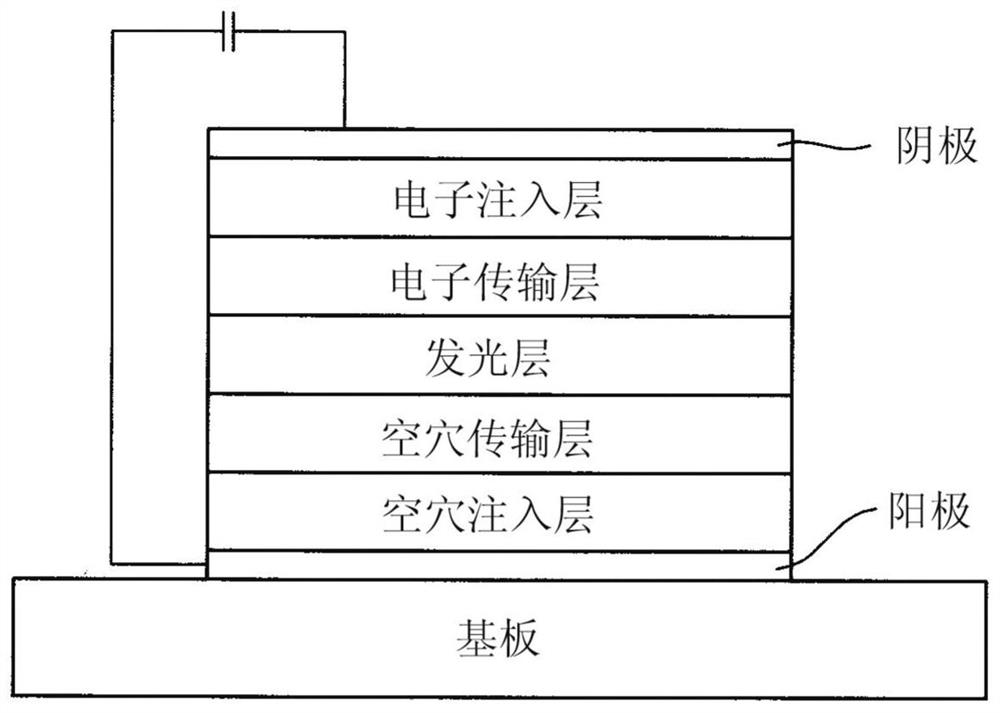
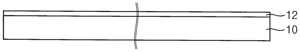
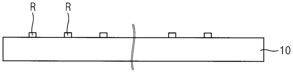
[0044] figure 1 It is a structural diagram of an organic light-emitting device. Figure 2a to Figure 2d It is a cross-sectional view of an organic light emitting display device for schematically illustrating formation of an organic light emitting structure of the organic light emitting display device.

[0045] refer to figure 1, the organic light-emitting element is sequentially stacked on the substrate to form an anode, a hole injection layer, a hole transfer layer, an emitting layer, and a hole blocking layer. ), electron transfer layer (electron transfer layer), electron injection layer (electron injection layer), cathode (cathode) and other films.

[0046] The organic thin film is composed of a multilayer of a hole injection layer, a hole transport layer, a light emitting layer, a hole blocking layer, an electron transport la...


PUM


Abstract

The invention discloses a laser etching device and a laser etching method using the same, comprising: a chamber, a substrate on which an organic film is formed, and a laser port is formed in the direction of the ground; a laser irradiator passes through the laser port and irradiating the organic film of the substrate with laser light; a particle trap, disposed in the chamber and on the laser port, and including a main body, an opening penetrating the main body and allowing the laser light to pass through and a capturing portion for capturing dust generated from the organic film; a thin film module including: a protective film disposed between the laser port and the particle trap so as not to be trapped by the particles The dust collector collects and passes through the dust accumulation of the particle collector, and is formed of a transparent substance; the film driving part can move the protective film.

Description

technical field [0001] The present invention relates to a laser etching device and a laser etching method using the laser etching device, in particular to a laser etching method for forming an organic light emitting structure of an organic light emitting display device. Background technique [0002] Recently, benefiting from the development of technology, display products with smaller size, lighter weight and higher performance are being produced. So far, among display devices, conventional cathode ray tube televisions (cathode ray tube: CRT) have been widely used because of their advantages in performance and price, but they can overcome the disadvantages of CRT in terms of miniaturization and portability. , and display devices with the advantages of miniaturization, light weight and low power consumption, such as plasma display devices, liquid crystal display devices, and organic light-emitting display devices, are attracting attention. [0003] Among them, organic electr...

Claims


Application Information

Patent Timeline
Patent Type & Authority Patents(China)
IPC IPC(8): H01L51/56
CPCH10K71/00H01L21/268H01L21/31138H10K71/211H10K71/231
Inventor 郑淏丞韩旼我
Owner SAMSUNG DISPLAY CO LTD
Why Eureka
Try Eureka