A Parallel Communication Method

A communication method and a technology of communication status, which are applied in the direction of instruments, electrical digital data processing, etc., can solve the problems of fewer timing links, more timing links, and fewer bus pins, so as to avoid logical conflicts, have fewer timing links, and read The effect of fast writing speed

Active Publication Date: 2020-06-09
深圳清时捷投资管理有限公司
View PDF5 Cites 0 Cited by
  • Summary
  • Abstract
  • Description
  • Claims
  • Application Information

AI Technical Summary

Problems solved by technology

To sum up, there are two constraints in this method. First, the MCU is mainly used for control, and pins are one of the most precious resources of the MCU. Usually there are not too many pins for communication; second, the MCU uses the program The method of controlling the I / O port to simulate the bus timing is not the concurrent timing generated by the real logic circuit, and it cannot strictly control the timing matching between signals
[0003] There are more or less problems when the existing parallel bus communicates, and three kinds of various chip-level communication parallel buses commonly used are given as examples: 1) as Figure 5 and Image 6 The PC ISA bus shown has 30 bus pins, including address bus: A0-A15, data bus: D0-D15, control bus: CS#, RD#, WR#, and its advantage lies in the timing link Less, the disadvantage is that the number of bus pins is large; 2) such as Figure 7 and Figure 8 The MCS-51 microcontroller bus shown has 20 bus pins, including address / data bus: AD0-AD15, control bus: ALE, CS#, RD#, WR#, and its advantage lies in the number of bus pins Relatively few, the disadvantage is that there are many timing links; 3) if Figure 9 and Figure 10 The MEBI bus of the HCS12 single-chip microcomputer shown has 18 bus pins, including address / data bus: AD0-AD15, control bus: ECLK, R / W#. Less, the disadvantage is that there is a logical conflict (gray part)

Method used


Image

  • A Parallel Communication Method
  • A Parallel Communication Method
  • A Parallel Communication Method

Examples


Embodiment Construction

[0041] In order to fully understand the technical content of the present invention, the technical solution of the present invention will be further introduced and illustrated below in conjunction with schematic diagrams, but is not limited thereto.

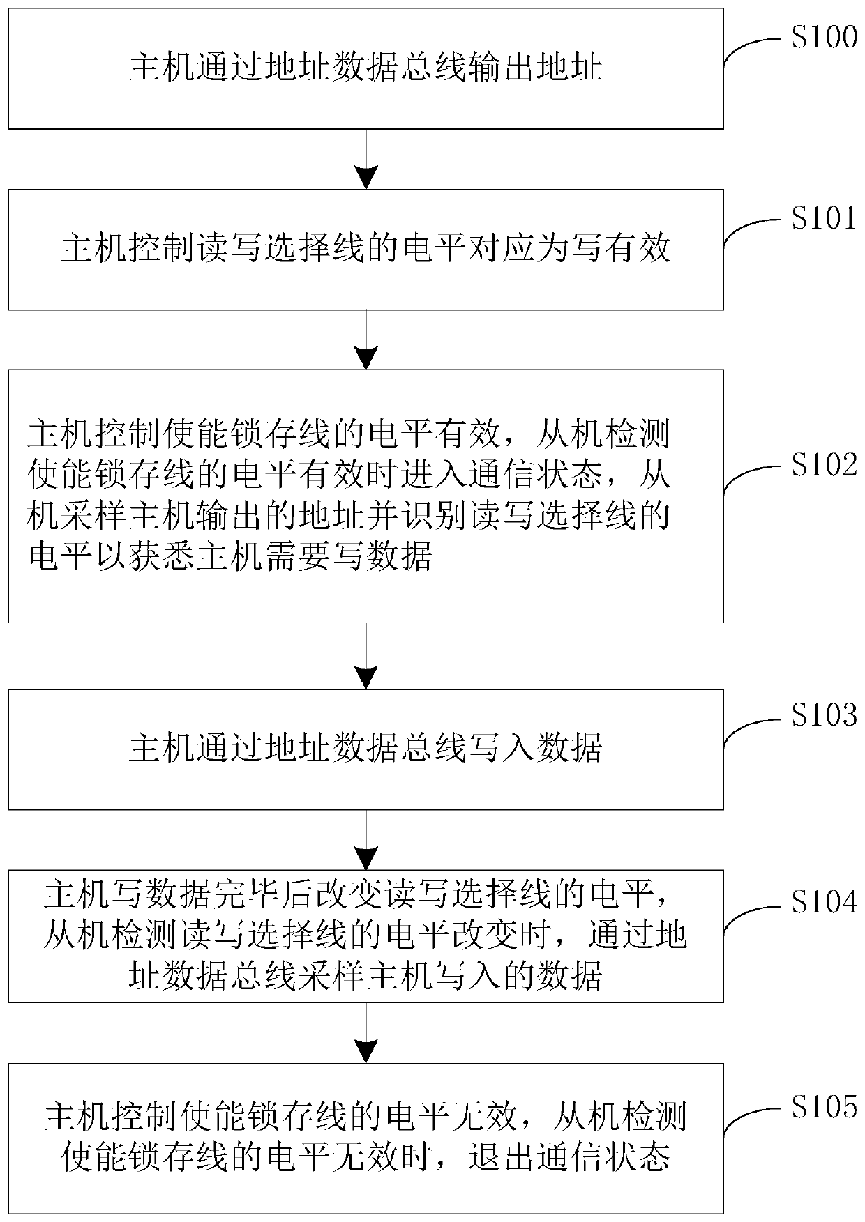
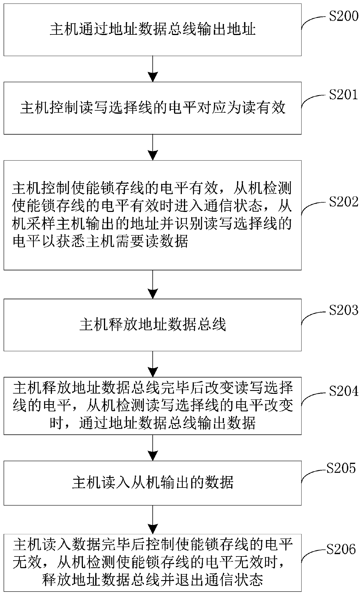
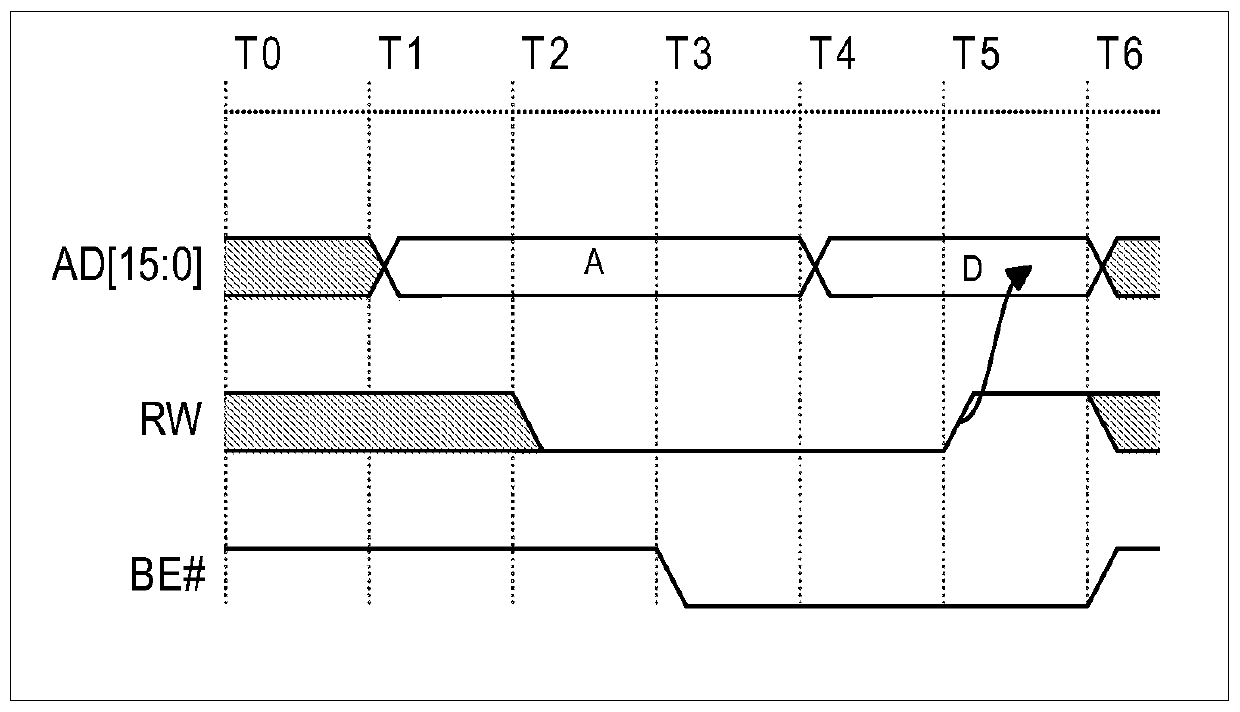
[0042] Such as Figure 1 to Figure 4As shown, in the present invention, the parallel communication method includes a bus connected between a master and a slave for parallel communication, and the bus includes an address data bus, a read / write selection line and an enable latch line. In this embodiment, the addressing space of the master is 64KB, and there are 16 address data buses, 1 read-write selection line and 1 enable latch line in the bus. The master and the slave are connected through these 18 lines. Can finish communication, its bus number is identical with the HCS12 single-chip microcomputer MEBI bus of the prior art, but it is less than the number of the PC machine ISA bus and the MCS-51 single-chip microcomputer bus of t...


PUM


Abstract

The invention discloses a parallel communication method. A bus for parallel communication is connected between a host computer and a slave computer and comprises an address data bus body, a reading-writing selection line and an enabling latching line; during communication, the host computer controls the level of the enabling latching line to be valid or invalid to get the slave computer into or out of the communication state; the host computer controls the level of the reading-writing selection line to enable the slave computer to learn that the host computer needs to write data or read data through the address data bus body; during data writing, the host computer changes the level of the reading-writing selection line to enable the slave computer to learn that the host computer completes data writing through the address data bus body so that written data output by the host computer can be input; during data reading, and the host computer changes the level of the reading-writing selection line to enable the slave computer to learn that the host computer completes releasing of the address data bus body so that read data can be output to the host computer. By means of the parallel communication method, the number of pins of the adopted host computer is small, the number of time sequence links is small, a time sequence is sufficient, logic conflicts are avoided, and user demands are met.

Description

technical field [0001] The invention relates to the field of digital circuit system communication, in particular to a parallel communication method. Background technique [0002] In recent years, many applications combine the master (such as MCU) with the slave (such as FPGA) to become the best partner. For example, MCU is responsible for low-speed functions such as system initialization, parameter and port configuration, and FPGA is responsible for high-speed functions such as data processing, access and transmission. Then the communication problem between MCU and FPGA becomes very prominent at this time. FPGA is a programmable device, the function of pins can be defined arbitrarily, and the number of pins is usually enough. Moreover, FPGA is essentially a kind of hardware, which can realize strict timing control. Therefore, the key point or bottleneck in designing the communication bus between MCU and FPGA lies in the characteristics of MCU. Since the existing MCU integ...

Claims


Application Information

Patent Timeline
Patent Type & Authority Patents(China)
IPC IPC(8): G06F13/42G06F13/40
CPCG06F13/4068G06F13/4204G06F2213/0004
Inventor 郑俭锋
Owner 深圳清时捷投资管理有限公司
Why Eureka
Try Eureka