Semiconductor junction temperature test device and test method thereof

A test device and semiconductor technology, applied in single semiconductor device testing, diode testing, etc., can solve the problems of inability to evaluate the real performance of semiconductors, probes that cannot be attached to the surface, and inaccurate temperature collection.

Active Publication Date: 2017-10-27
YANGZHOU YANGJIE ELECTRONIC TECH CO LTD
View PDF8 Cites 7 Cited by
  • Summary
  • Abstract
  • Description
  • Claims
  • Application Information

AI Technical Summary

Problems solved by technology

The disadvantages of this method are: 1. To test the shell temperature Tc of the product, the temperature-sensing probe needs to be close to the surface of the product, so that the temperature generated by the forward power consumption can be accurately reflected to the test instrument, but in practice, the probe often cannot It is close to the surface, and the higher the temperature, the easier it is for the probe to loosen, and the more inaccurate the temperature collection; 2. The thermal resistance value is tested by the supplier and explained to the customer through the specification. There are often large differences in the thermal resistance value of different manufacturers of similar products. Among them There are not only the subjective factors of the supplier, but also the reason why the thermal resistance value itself has a large error in the test process (including the collection of shell temperature, etc.)
But its essence is to use multiple sampling to get the corresponding calculation formula, and finally get the junction temperature of the semiconductor through the calculation method, which is a theoretical value, not an actual measurement value, so the junction temperature calculated in this way is the same as that of the semiconductor PN junction in the actual working state. The difference in junction temperature is large, and the real performance of semiconductors cannot be evaluated

Method used


Image

  • Semiconductor junction temperature test device and test method thereof
  • Semiconductor junction temperature test device and test method thereof

Examples


Embodiment Construction

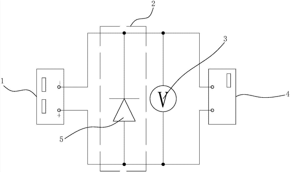
[0034] As shown in the figure, the present invention is a semiconductor junction temperature testing device, which includes a diode installation position 5 and a constant current source 1, the diode installation position 5 is connected to the constant current source 1, and a voltmeter 3 is connected in parallel at both ends of the diode installation position, The diode placement is set in the oven 2; it also includes a semiconductor characteristic tester 4, the semiconductor characteristic tester is connected in parallel to both ends of the diode placement, and a diode is arranged on the diode placement. When in use, place the semiconductor diode on the diode placement position, use a constant current source to provide a constant current, and the oven provides a stable ambient temperature. When the semiconductor diode is placed in the oven for a long enough time, the junction temperature of the semiconductor diode is consistent with the temperature of the oven. At this time, th...


PUM


Abstract

The invention provides a semiconductor junction temperature test device and a test method thereof, relates to the electronic device test field and especially relates to the semiconductor junction temperature test device and the test method thereof, and provides the semiconductor junction temperature test device and the test method thereof, which can directly measure the semiconductor junction temperature, are small in error of the measured junction temperature and can truly reflect real performance of a semiconductor diode. The test device comprises a diode mounting place and a constant current source, wherein the diode mounting place is connected with the constant current source. The test device also comprises a semiconductor characteristic tester. The semiconductor characteristic tester is connected in parallel to the two ends of the diode mounting place; and the diode mounting place is provided with a diode. The diode mounting place comprises an insulated base. The base is provided with a pair of clamp places; and wiring ends of the diode are clamped in the clamp places correspondingly. The semiconductor junction temperature test device and the test method thereof have the advantages of being capable of directly measuring the semiconductor junction temperature, being small in error of the measured junction temperature and being capable of truly reflecting the real performance of the semiconductor diode.

Description

technical field [0001] The invention relates to the field of electronic device testing, in particular to a semiconductor junction temperature testing device and a testing method thereof. Background technique [0002] A semiconductor device is an electronic device with unidirectional conductivity. It is characterized in that it can realize the functions of forward conduction and reverse cut-off in the circuit. It is the basic component of large-scale integrated circuits and occupies a very important position in the field of electronics industry. . It is well known that the characteristics of semiconductors are related to the degree of carrier excitation in the PN junction, and temperature is the most important factor affecting the degree of carrier excitation, and is the key to determining whether the semiconductor device can work normally. Therefore, the junction temperature test has become the first test item to be done in the new product verification and application selec...

Claims


Application Information

Patent Timeline
Patent Type & Authority Applications(China)
IPC IPC(8): G01R31/26
CPCG01R31/2632
Inventor 景昌忠杨毓敏吴云云陈斌刘宁王欢王晶王毅
Owner YANGZHOU YANGJIE ELECTRONIC TECH CO LTD
Why Eureka
Try Eureka