
Faraday shield and reaction chamber

A Faraday shielding and reaction chamber technology, applied to electrical components, discharge tubes, circuits, etc., can solve problems such as high temperature and increase the risk of particle contamination in the reaction chamber 1, so as to avoid excessive temperature and reduce Risk of particle contamination, effect of increasing overall coupling efficiency

Pending Publication Date: 2017-10-27
BEIJING NAURA MICROELECTRONICS EQUIP CO LTD
View PDF9 Cites 3 Cited by
  • Summary
  • Abstract
  • Description
  • Claims
  • Application Information

AI Technical Summary

Problems solved by technology

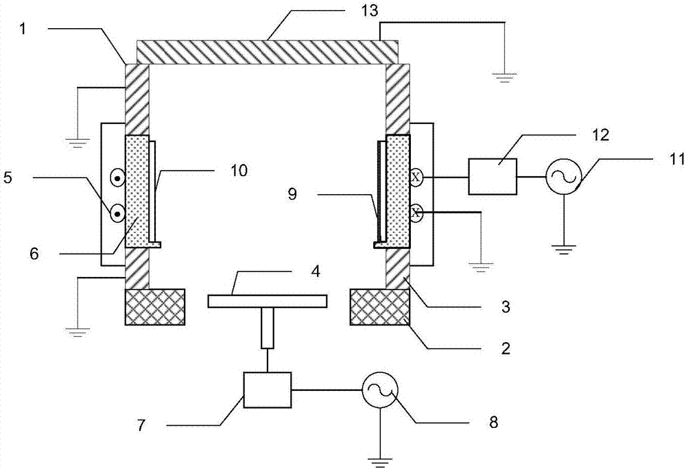
However, loading the RF coil 4 with high RF power will cause the Faraday shield 10 to overheat due to eddy current losses and ion bombardment, thereby increasing the risk of particle contamination of the reaction chamber 1

Method used


Image

  • Faraday shield and reaction chamber
  • Faraday shield and reaction chamber
  • Faraday shield and reaction chamber

Examples


Embodiment Construction

[0055] In order for those skilled in the art to better understand the technical solution of the present invention, the Faraday shield and the reaction chamber provided by the present invention will be described in detail below with reference to the accompanying drawings.

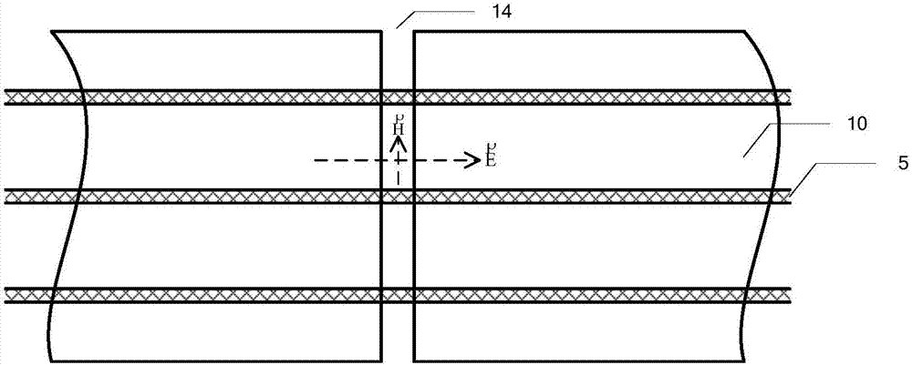
[0056] Please also refer to Figure 4A with Figure 4B , the Faraday shield provided by the first embodiment of the present invention includes a conductive ring body 11, and a slit is formed on the conductive ring body 11, and the slit includes a first sub-slit 111, and the first sub-slit 111 It is arranged along the circumferential direction of the conductive ring body, and forms an included angle a with the axis of the conductive ring body 11 . The electromagnetic field generated by the radio frequency coil 13 surrounding the conductive ring 11 can be divided into a magnetic field component A in the axial direction of the conductive ring 11 and an electric field component B in the circumferential directio...


PUM


Abstract

The present invention provides a Faraday shield and a reaction chamber, comprising a conductive ring body and a slit formed in the conductive ring body. The slit includes a first sub-slit which is arranged along the circumferential direction of the conductive ring body and forms an included angle with the axis of the conductive ring body for increasing the total coupling efficiency of the electromagnetic field by increasing the coupling efficiency of the electric field component of the electromagnetic field in the circumferential direction of the conductive ring body. The Faraday shield provided by the invention can improve the coupling efficiency of the electric field to reduce the radio frequency power loaded on the radio frequency coil.

Description

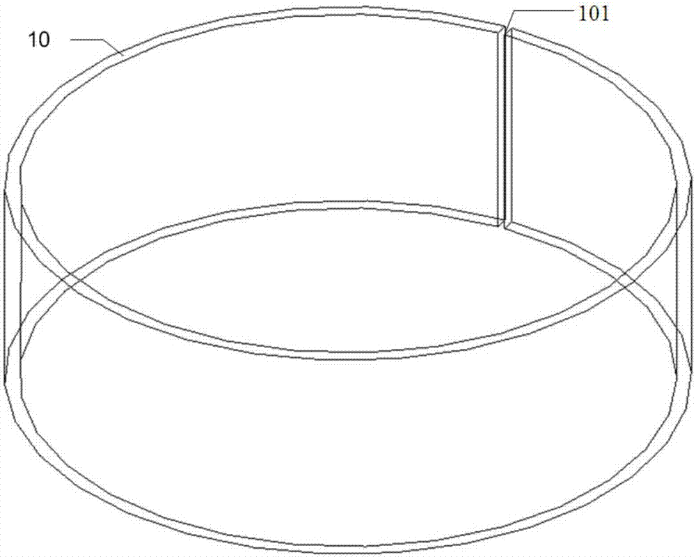
technical field [0001] The invention relates to the technical field of semiconductor manufacturing, in particular to a Faraday shield and a reaction chamber. Background technique [0002] In the process of using Inductive Coupled Plasma (Inductive Coupled Plasma Emission Spectrometer, hereinafter referred to as ICP) device for the manufacturing process of integrated circuits and MEMS devices, the generated plasma contains a large number of electrons, ions, excited atoms, molecules and free These active particles interact with the substrate to cause various physical and chemical reactions on the surface of the material, thereby changing the surface properties of the material. [0003] figure 1 It is a cross-sectional view of a conventional ICP device. see figure 1 , The ICP device includes a reaction chamber 1 , and a medium cartridge 3 is arranged on the side wall 2 of the reaction chamber 1 . A radio frequency coil 4 is arranged around the outer side of the dielectric c...

Claims


Application Information

Patent Timeline
Patent Type & Authority Applications(China)
IPC IPC(8): H01J37/32
CPCH01J37/321H01J37/32431H01J37/32651H01J37/32798
Inventor 刘建生陈鹏王文章常大磊徐奎丁培军姜鑫先张璐苏振宁宋巧丽贾强
Owner BEIJING NAURA MICROELECTRONICS EQUIP CO LTD
Learn More