Image sensor structure and preparation method thereof
An image sensor and structure layer technology, applied in the field of image sensors, can solve the problems affecting the detection sensitivity of infrared image sensors, the difference in thermal noise between blind element arrays and pixel arrays, etc., so as to improve chip integration and device sensitivity, and reduce detection. error, the effect of improving detection sensitivity
- Summary
- Abstract
- Description
- Claims
- Application Information
AI Technical Summary
Problems solved by technology
Method used
Image

Examples
Embodiment 1
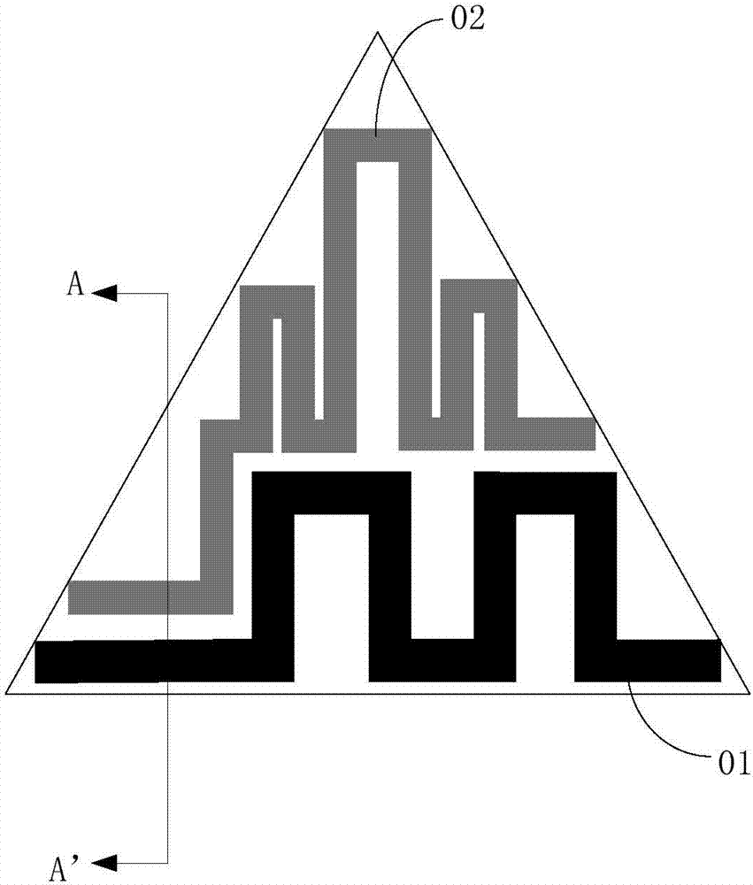
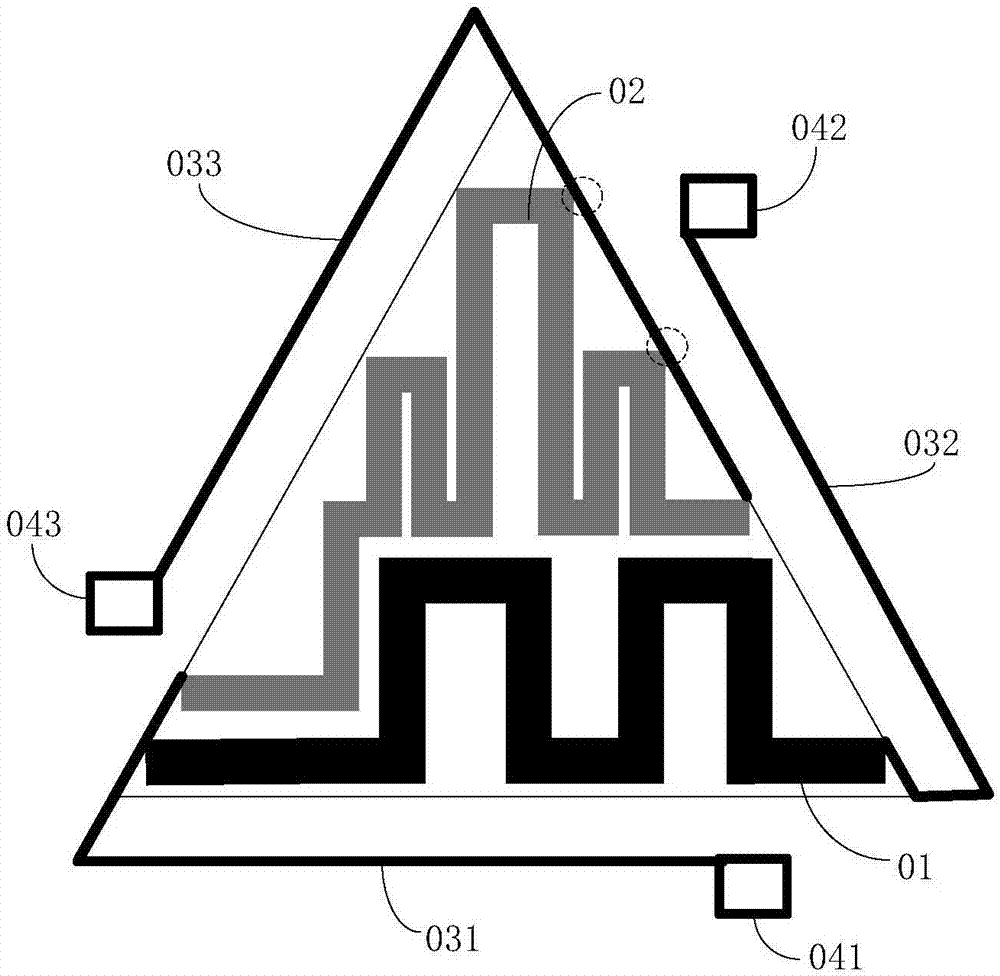
[0033] The following is attached Figure 1-12 The present invention will be described in further detail with specific examples. in, figure 1 , 3 The thin-line triangles in sums 6-12 indicate that the effective pixel is approximately triangular in shape, but this is not used to limit the protection scope of the present invention. It should be noted that the drawings are all in a very simplified form, using imprecise scales, and are only used to facilitate and clearly achieve the purpose of assisting in describing the present embodiment.
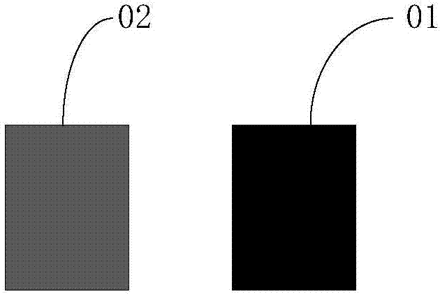
[0034] see figure 1 and figure 2 , figure 2 for figure 1 Schematic diagram of the cross-sectional structure along the AA' direction. In an image sensor structure of this embodiment, each effective pixel in the effective pixel array includes: a detection structure layer 01 and a blind cell structure layer 02 . Here, the detection structure layer 01 and the blind cell structure layer 02 are arranged side by side, and of course they can...
Embodiment 2
[0047] The following is attached Figures 13 to 23 The present invention will be described in further detail with specific examples. in, Figure 13 The thin line triangles in the mean that the shape of the effective pixel is approximately triangular, and, in order to clearly express the morphology of the detection structure layer and the blind cell structure layer, the concave part of the blind cell structure layer is represented as white, but this is not used to limit this protection scope of the invention. It should be noted that the drawings are all in a very simplified form, using imprecise scales, and are only used to facilitate and clearly achieve the purpose of assisting in describing the present embodiment.
[0048] see Figures 13 to 15 The difference between the effective pixel in the second embodiment and the effective pixel in the first embodiment is that a blind pixel structure layer 202 is arranged inside the surface of the detection structure layer 201 instea...
Embodiment 3
[0059] The following is attached Figures 24 to 29 The present invention will be described in further detail with specific examples. It should be noted that the drawings are all in a very simplified form, using imprecise scales, and are only used to facilitate and clearly achieve the purpose of assisting in describing the present embodiment.
[0060] The difference between the third embodiment and the first and second embodiments is that the detection structure layer and the blind element structure layer are stacked up and down. Specifically, see Figure 26 , in the effective pixel structure, the blind pixel structure layer 302 is located on the sidewall and top of the detection structure layer 301 , that is, the blind pixel structure layer 302 covers the detection structure layer 301 . the following Figure 24 and 25 for Figure 19 The enlarged cross-sectional schematic diagram of the area shown by the dotted circle in , at this time, the preparation of the blind cell st...
PUM
 Abstract
Description
Claims
Application Information
 - R&D
- Intellectual Property
- Life Sciences
- Materials
- Tech Scout
- Unparalleled Data Quality
- Higher Quality Content
- 60% Fewer Hallucinations
Browse by: Latest US Patents, China's latest patents, Technical Efficacy Thesaurus, Application Domain, Technology Topic, Popular Technical Reports.
© 2025 PatSnap. All rights reserved.Legal|Privacy policy|Modern Slavery Act Transparency Statement|Sitemap|About US| Contact US: help@patsnap.com