Phototransistor based on ferroelectric gate dielectric and thin layer MoS2 channel

A phototransistor and gate dielectric technology, applied in circuits, electrical components, semiconductor devices, etc., can solve problems such as poor mechanical and thermal stability, slow ferroelectric domain inversion rate, high coercive field strength, etc., and achieve high residual Effects of polarization, enhanced transmittance, and low coercive field strength

Inactive Publication Date: 2017-11-10
CHONGQING UNIV
View PDF3 Cites 22 Cited by
  • Summary
  • Abstract
  • Description
  • Claims
  • Application Information

AI Technical Summary

Problems solved by technology

However, the organic ferroelectric material P(VDF-TrFE) has the following insurmountable disadvantages: slow ferroelectric domain inversion rate, high coercive field strength, poor mechanical and thermal stability, and is not compatible with micro Electronic Process Compatible

Method used


Image

  • Phototransistor based on ferroelectric gate dielectric and thin layer MoS2 channel
  • Phototransistor based on ferroelectric gate dielectric and thin layer MoS2 channel

Examples


Embodiment Construction

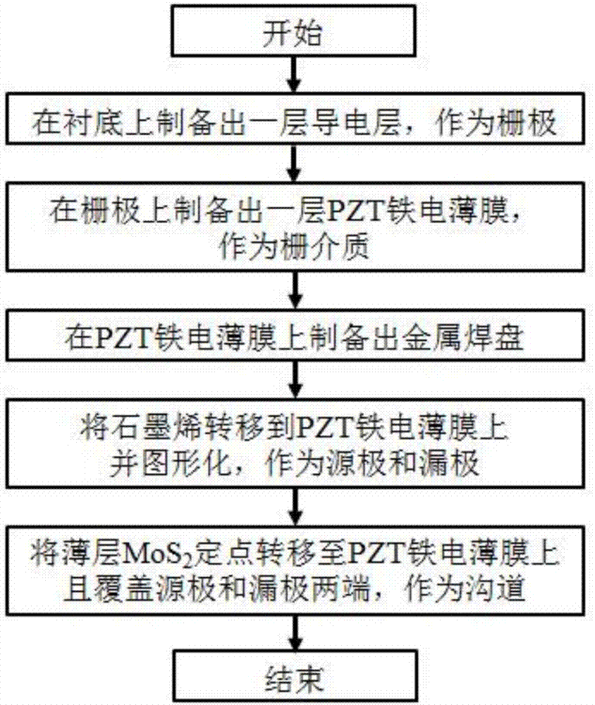
[0017] In order to make the content of the present invention more clearly understood, the present invention will be further described below in conjunction with the accompanying drawings according to specific embodiments.

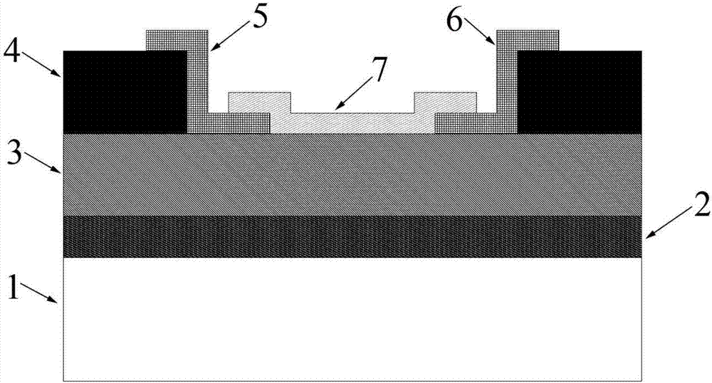
[0018] refer to figure 2 , a graphene-based electrode, PZT ferroelectric film gate dielectric and thin-layer MoS 2 The channel phototransistor mainly includes a substrate 1 , a gate 2 , a gate dielectric 3 , a metal pad 4 , a source 5 , a drain 6 and a channel 7 . Among them, the substrate 1 is SiO 2 / Si or SrTiO 3 substrate, the gate 2 is metal (for example, Ti / Pt) or conductive oxide (for example, SrRuO 3 ), the gate dielectric 3 is a PZT ferroelectric thin film, the source 5 and drain 6 are graphene (about 1-30 layers thick), and the channel 7 is a thin layer (1-30 layers) MoS 2 . The phototransistor is a back-gate structure, that is, a thin layer of MoS 2 The channel 7 is located on the upper surface of the PZT ferroelectric thin film gate dielect...


PUM


Abstract

The invention belongs to the field of micro-nano semiconductor optoelectronic devices, and particularly relates to a phototransistor based on a ferroelectric gate dielectric and a thin layer MoS2 channel and a preparation method thereof. The phototransistor comprises a source electrode, a leakage electrode, a channel, a gate electrode, a gate dielectric, a metal pad, and a substrate. The source electrode and the leakage electrode are graphene, the channel is thin layer MoS2, and the gate dielectric is a PZT ferroelectric membrane. Compared with existing similar phototransistor, the phototransistor has the following advantages that first, a high dielectric coefficienet of the PZT ferroelectric membrane helps improve the adjustment performance of the gate electrode for a channel carrier; second, the PZT ferroelectric membrane can adjust the channel carrier with surplus polarity field strength, so that the power consumption of the device is lowered; third, compared with organic ferroelectric material P (VDF-TrFE), the PZT ferroelectric membrane has the advantages of high surplus polarity, low coercive field strength, stable property and compatibility with microelectronic process; and fourth, as the source electrode and leakage electrode, the graphene can improve the signal light transmittance, and improve the light response degree and gain of the device.

Description

technical field [0001] The invention belongs to the field of micro-nano semiconductor optoelectronic devices, in particular to a graphene electrode, lead zirconate titanate (PZT, PbZr x Ti (1-x) o 3 ) ferroelectric thin film gate dielectric and thin molybdenum disulfide (MoS 2 ) channel phototransistor and its preparation method. Background technique [0002] Photodetectors are a class of devices that convert optical signals into electrical signals, and are widely used in sensing, imaging, display, and optical communication. Photodetectors can be roughly divided into three categories according to their working principles: photoconductive type, photodiode type, and phototransistor type. Photoconductive photodetectors are composed of semiconductor materials and ohmic contacts at both ends, and have the advantages of high gain and simple structure. Photodiode photodetectors are usually composed of p-n junctions, p-i-n junctions or Schottky structures, which have the advant...

Claims


Application Information

Patent Timeline
Patent Type & Authority Applications(China)
IPC IPC(8): H01L31/113H01L31/0224H01L31/032H01L31/18
CPCH01L31/022408H01L31/032H01L31/1136H01L31/18Y02P70/50
Inventor 金伟锋牟笑静尚正国王婧文
Owner CHONGQING UNIV
Why Eureka
Try Eureka