
A three-dimensional memory electromigration test structure and its manufacturing method

A technology of test structure and manufacturing method, which is applied in the direction of semiconductor/solid-state device test/measurement, circuit, electrical components, etc., can solve the problems of test result deviation, test structure damage, etc., achieve fast and accurate positioning, realize precise positioning, and improve positioning the effect of time

Active Publication Date: 2019-11-26
YANGTZE MEMORY TECH CO LTD
View PDF6 Cites 0 Cited by
  • Summary
  • Abstract
  • Description
  • Claims
  • Application Information

AI Technical Summary

Problems solved by technology

[0005] In view of this, the present invention provides a three-dimensional memory electromigration test structure and its manufacturing method to solve the problem in the prior art that the test structure is damaged during the positioning process, resulting in deviations in test results

Method used


Image

  • A three-dimensional memory electromigration test structure and its manufacturing method
  • A three-dimensional memory electromigration test structure and its manufacturing method
  • A three-dimensional memory electromigration test structure and its manufacturing method

Examples


Embodiment Construction

[0046] As mentioned in the background technology section, the positioning method of the test line in the prior art is easy to cause damage to the test structure, which in turn causes deviations in the test results during the test process.

[0047]Specifically, since the main structure of the test line and the virtual line is the same, there is no big difference, so there is no way to locate the test line through the structural difference, and the test line must be located by setting a mark.

[0048] During the sample preparation process of the electromigration test structure, an oxide layer of tens of nanometers to a hundred nanometers must be reserved above the upper metal line M02 to avoid loss of the test line T01 in the M02 during the preparation of the FIB sample. Limited by the observation depth (<200nm) of SEM (Scanning Electron Microscope, scanning electron microscope), the thicker the oxide layer is, the less clear the image will be. Coupled with the fact that the wid...


PUM


Abstract

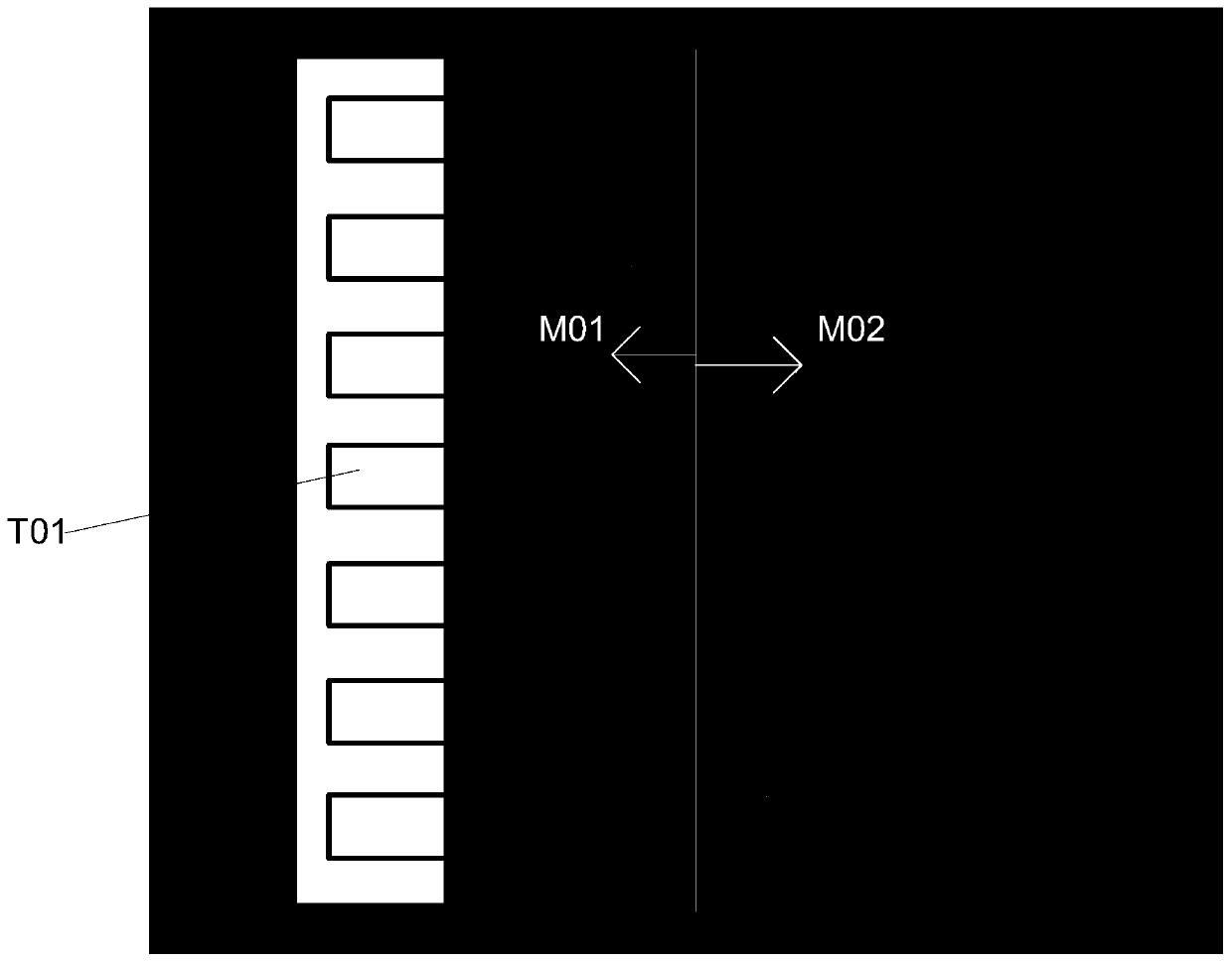
The invention provides a three-dimensional memory electromigration test structure and the manufacturing method thereof. In an electromigration test structure manufacturing process, Markers are made on oxide layers of a first virtual line and a second virtual line adjacent to a test line to position the test line. Since markers are made on the oxide layers of the first virtual line and the second virtual line on the two sides of the test line, the metallic line in the middle of markers can be directly positioned as the test line during making an electromigration test structure sample, and rapid and accurate position of the test line can be realized. An electromigration test structure sample can be obtained by cutting the two sides of the test line. Since the markers are on the oxide layers of the first virtual line and the second virtual line, the test line may not be affected, and accurate position of the test line can be realized without damaging the test line and a first metallic line connected with the test line. Sample making success rate is greatly improved, and the positioning time of test line can be shortened.

Description

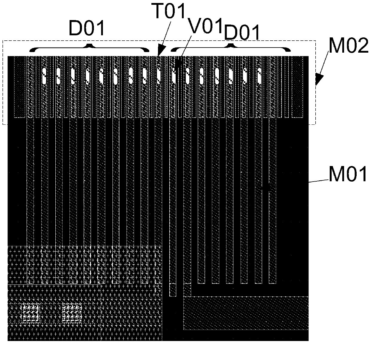
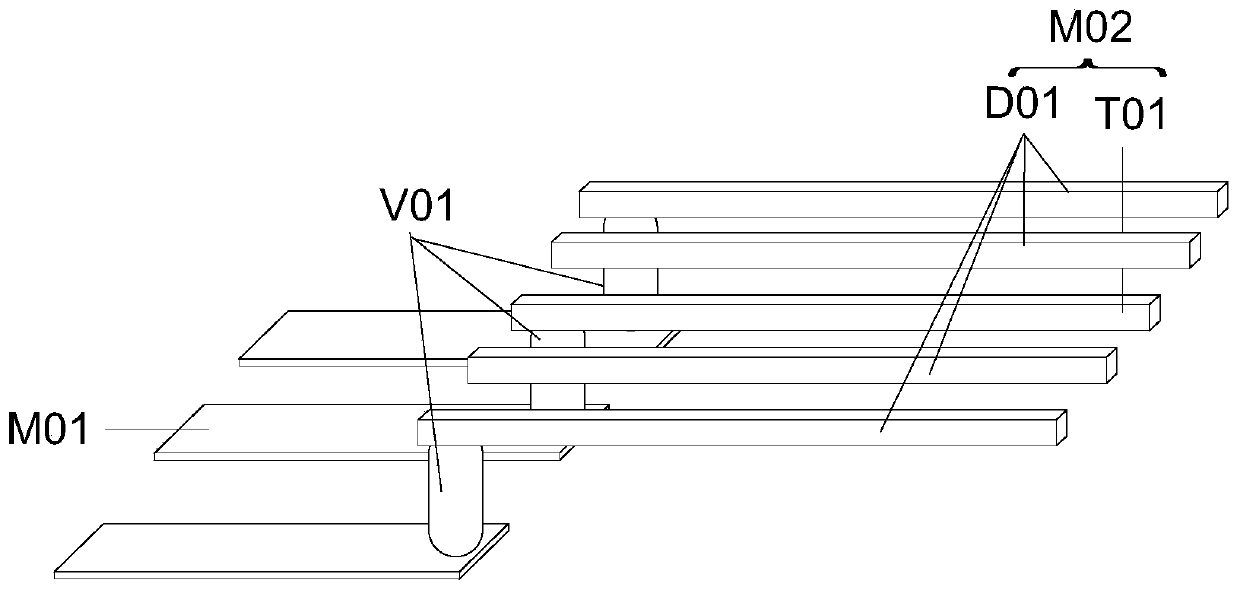
technical field [0001] The invention relates to the technical field of manufacturing semiconductor devices, in particular to a three-dimensional memory electromigration test structure and a manufacturing method thereof. Background technique [0002] NAND flash memory is a better storage device than hard disk drives, and it has been widely used in electronic products as people pursue non-volatile storage products with low power consumption, light weight and high performance. At present, the planar NAND flash memory is close to the limit of practical expansion. In order to further increase the storage capacity and reduce the storage cost per bit, a 3D NAND memory, that is, 3D NAND, is proposed. [0003] The current 3D NAND M2DP_EM test key (double exposure metal line 2 electromigration test structure) such as figure 1 with figure 2 The design shown, where, figure 1 It is a schematic top view of the three-dimensional memory electromigration test structure; figure 2 It is ...

Claims


Application Information

Patent Timeline
Patent Type & Authority Patents(China)
IPC IPC(8): H01L23/544
CPCH01L22/34H01L23/544H01L2223/54433
Inventor 蔚倩倩郭伟仝金雨李桂花李辉
Owner YANGTZE MEMORY TECH CO LTD
Learn More