Top-emission AMOLED pixel circuit and driving method thereof

一种像素电路、驱动方法的技术,应用在顶发射AMOLED像素电路及其驱动领域,能够解决电路失效等问题,达到缓解IR压降、解决VSS电压抬升的效果

Active Publication Date: 2017-11-24
SHENZHEN CHINA STAR OPTOELECTRONICS SEMICON DISPLAY TECH CO LTD
View PDF8 Cites 10 Cited by
  • Summary
  • Abstract
  • Description
  • Claims
  • Application Information

AI Technical Summary

Problems solved by technology

[0007] Therefore, the object of the present invention is to provide a top-emitting AMOLED pixel circuit to solve the problem of circuit failure caused by the low power supply voltage VSS voltage rise
[0008] Another object of the present invention is to provide a driving method for a top-emitting AMOLED pixel circuit, which solves the problem of circuit failure caused by the low power supply voltage VSS voltage rise

Method used


Image

  • Top-emission AMOLED pixel circuit and driving method thereof
  • Top-emission AMOLED pixel circuit and driving method thereof
  • Top-emission AMOLED pixel circuit and driving method thereof

Examples


Embodiment Construction

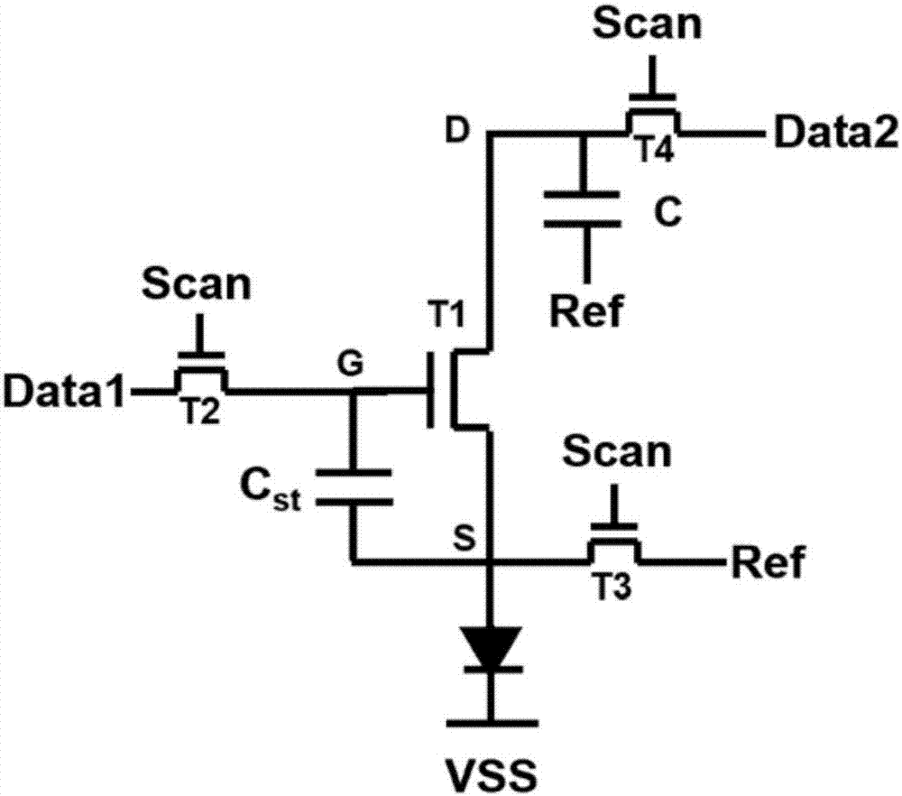
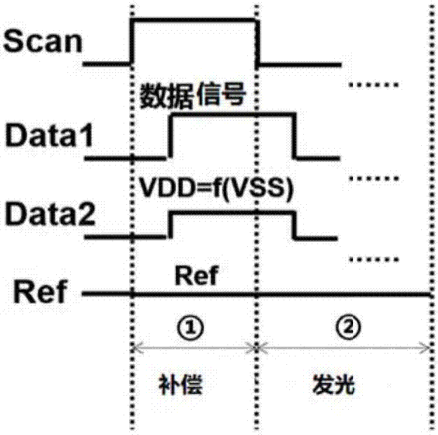
[0034] see figure 2 and image 3 , figure 2 It is a schematic circuit diagram of a preferred embodiment of the top emission AMOLED pixel circuit of the present invention, image 3 It is a schematic diagram of the signal sequence of this preferred embodiment. This preferred embodiment is a 4T2C pixel circuit, which mainly includes thin film transistors T1~T4, capacitors Cst and C, where T1 is a driving TFT: the gate of T1 is connected to node G, the source and The drain is connected to nodes S and D respectively; the gate of T2 is connected to the scan signal Scan, the source and drain are respectively connected to node G and the data signal Data1; the gate of T3 is connected to the scan signal Scan, and the source and drain are respectively connected to node S and the reference Voltage Ref; the gate of T4 is connected to the scanning signal Scan, the source and the drain are respectively connected to node D and the high voltage of the power supply (Data2; the two ends of t...


PUM


Abstract

The invention relates to a top-emission AMOLED pixel circuit and a driving method thereof; the top-emission AMOLED pixel circuit comprises the following units: a first film transistor (T1) connected with a first node (G), a second node (S) and a third node (D); a second film transistor (T2) connected with a scan signal (Scan), the first node (G) and a data signal (Data1); a third film transistor (T3) connected with the scan signal (Scan), the second node (S) and a reference voltage (Ref); a fourth film transistor (T4) connected with the scan signal (Scan), the third node (D) and a power supply high voltage (Data2); a first capacitor (Cst) connected with the first node (G) and the second node (S); a second capacitor (C) connected with the third node (D) and the reference voltage (Ref); an OLED connected with the second node (S) and a power supply low voltage (VSS); the difference between the power supply high voltage (Data2) and the power supply low voltage (VSS) remains unchanged. The invention also provides the corresponding driving method. The top-emission AMOLED pixel circuit and the driving method thereof can effectively alleviate IR voltage drop caused by the transparency cathode impedance increases.

Description

technical field [0001] The invention relates to the field of display technology, in particular to a top-emitting AMOLED pixel circuit and a driving method thereof. Background technique [0002] As a new generation of display technology, organic light-emitting diode (OLED) display panels have the advantages of low power consumption, high color gamut, high brightness, high resolution, wide viewing angle, and high response speed, so they are favored by the market. [0003] OLED display devices can be classified into two types according to their driving methods: passive matrix OLED (Passive Matrix OLED, PMOLED) and active matrix OLED (Active Matrix OLED, AMOLED). Among them, AMOLED has pixels arranged in an array, belongs to the active display type, has high luminous efficiency, and is usually used as a high-definition large-size display device. OLED can be divided into two structures according to the direction of light emission: one is the bottom emission type, and the other i...

Claims


Application Information

Patent Timeline
Patent Type & Authority Applications(China)
IPC IPC(8): G09G3/3233
CPCG09G3/3233G09G3/3266G09G2300/0819G09G2300/0842G09G2300/0866H10K2102/3026G09G2300/0852G09G2300/0861G09G2320/045G09G2320/043G09G3/3258G09G2320/0204H01L27/1225H01L29/78672H01L29/7869H10K59/1213
Inventor 韩佰祥
Owner SHENZHEN CHINA STAR OPTOELECTRONICS SEMICON DISPLAY TECH CO LTD
Why Eureka
Try Eureka