Packaging method of OLED display panel

A packaging method and display panel technology, applied in the manufacture of electrical components, electrical solid devices, semiconductor/solid devices, etc., can solve the problems of electrostatic damage, film layer structure damage, high cost, etc., to save costs, increase reliability, The effect of avoiding static electricity injury

Inactive Publication Date: 2017-11-28
WUHAN CHINA STAR OPTOELECTRONICS SEMICON DISPLAY TECH CO LTD
View PDF3 Cites 8 Cited by
  • Summary
  • Abstract
  • Description
  • Claims
  • Application Information

AI Technical Summary

Problems solved by technology

[0007] The purpose of the present invention is to provide a packaging method for OLED display panels, which can effectively solve the problems of electrostatic damage, film structure damage and particles caused by the use of masks in the existing thin film packaging process without using masks. problems, increases the reliability of inorganic barrier layers, and saves expensive mask costs

Method used


Image

  • Packaging method of OLED display panel
  • Packaging method of OLED display panel
  • Packaging method of OLED display panel

Examples


Embodiment Construction

[0032] In order to further illustrate the technical means and effects adopted by the present invention, the following describes in detail in conjunction with preferred embodiments of the present invention and accompanying drawings.

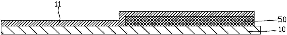
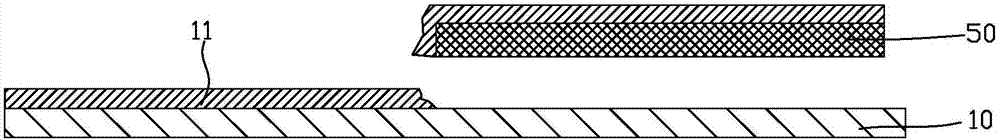
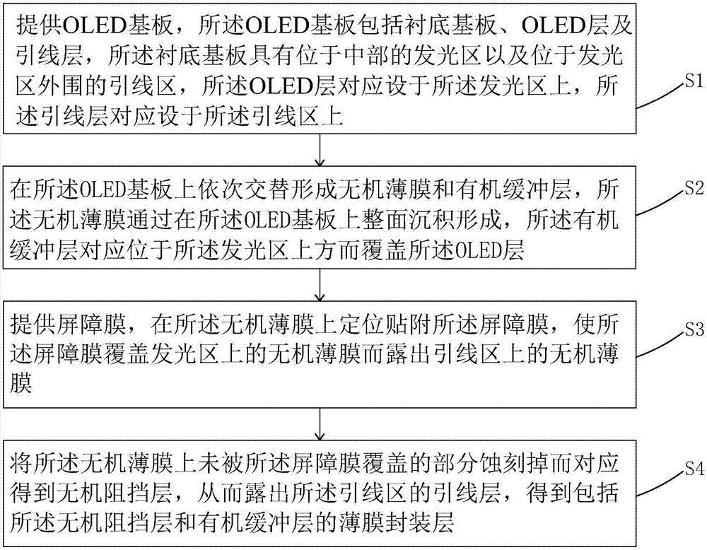
[0033] see image 3 , the present invention provides a method for encapsulating an OLED display panel, comprising the following steps:

[0034] Step S1, such as Figure 4 As shown, an OLED substrate 100 is provided. The OLED substrate 100 includes a base substrate 101, an OLED layer 102, and a lead layer 103. The base substrate 101 has a light-emitting area located in the middle and a lead area located at the periphery of the light-emitting area. The OLED layer 102 is correspondingly disposed on the light-emitting area of ​​the base substrate 101 , and the lead layer 103 is correspondingly disposed on the lead area of ​​the base substrate 101 and connected to the OLED layer 102 .

[0035] Specifically, the base substrate 101 is a glass substrate...


PUM


Abstract

The invention provides a packaging method of an OLED display panel. Firstly whole-surface deposition is performed on an OLED substrate for forming an inorganic film. Then a barrier film is adhered on the inorganic film so that the barrier film covers the inorganic film on a light emitting area and the inorganic film on a lead area is exposed. Finally the barrier film is used as a shielding layer. The part which is not converted by the barrier film on the inorganic film is etched and an inorganic blocking layer of a film packaging layer is correspondingly obtained. According to the packaging method, the barrier film is used for etching the inorganic film for obtaining the patterned inorganic blocking layer, and no mask plate is required, thereby preventing a static damage problem caused by the mask plate, a film layer structure damage problem and a particle problem caused by film layer tearing in a separation process between the mask plate and the OLED substrate. The packaging method improves reliability of the inorganic blocking layer and can save a high expense of the mask plate.

Description

technical field [0001] The invention relates to the field of flat panel display technology, in particular to a packaging method for an OLED display panel. Background technique [0002] Organic Light-Emitting Diode (OLED) displays have the characteristics of self-illumination, high brightness, wide viewing angle, high contrast, flexibility, and low energy consumption. Has begun to gradually replace the traditional liquid crystal display. At present, the application of OLED display panels has become a high-end symbol from small-sized mobile phone display screens to large-sized high-resolution flat-panel TVs. [0003] Unlike traditional liquid crystal display technology, OLED display technology does not require a backlight, and uses very thin coatings of organic materials and glass substrates that emit light when an electric current passes through them. However, because organic materials are easy to react with water vapor or oxygen, as a display device based on organic materi...

Claims


Application Information

Patent Timeline
Patent Type & Authority Applications(China)
IPC IPC(8): H01L51/56H01L51/52
CPCH10K50/8445H10K71/00
Inventor 王杲祯余威
Owner WUHAN CHINA STAR OPTOELECTRONICS SEMICON DISPLAY TECH CO LTD
Why Eureka
Try Eureka