

Backlight unit and display device comprising same
A backlight unit, a single technology, applied in optics, nonlinear optics, instruments, etc., can solve problems such as poor uniformity of light emission and thick thickness
- Summary
- Abstract
- Description
- Claims
- Application Information
AI Technical Summary
Problems solved by technology
Method used
Image

Examples
Embodiment 1
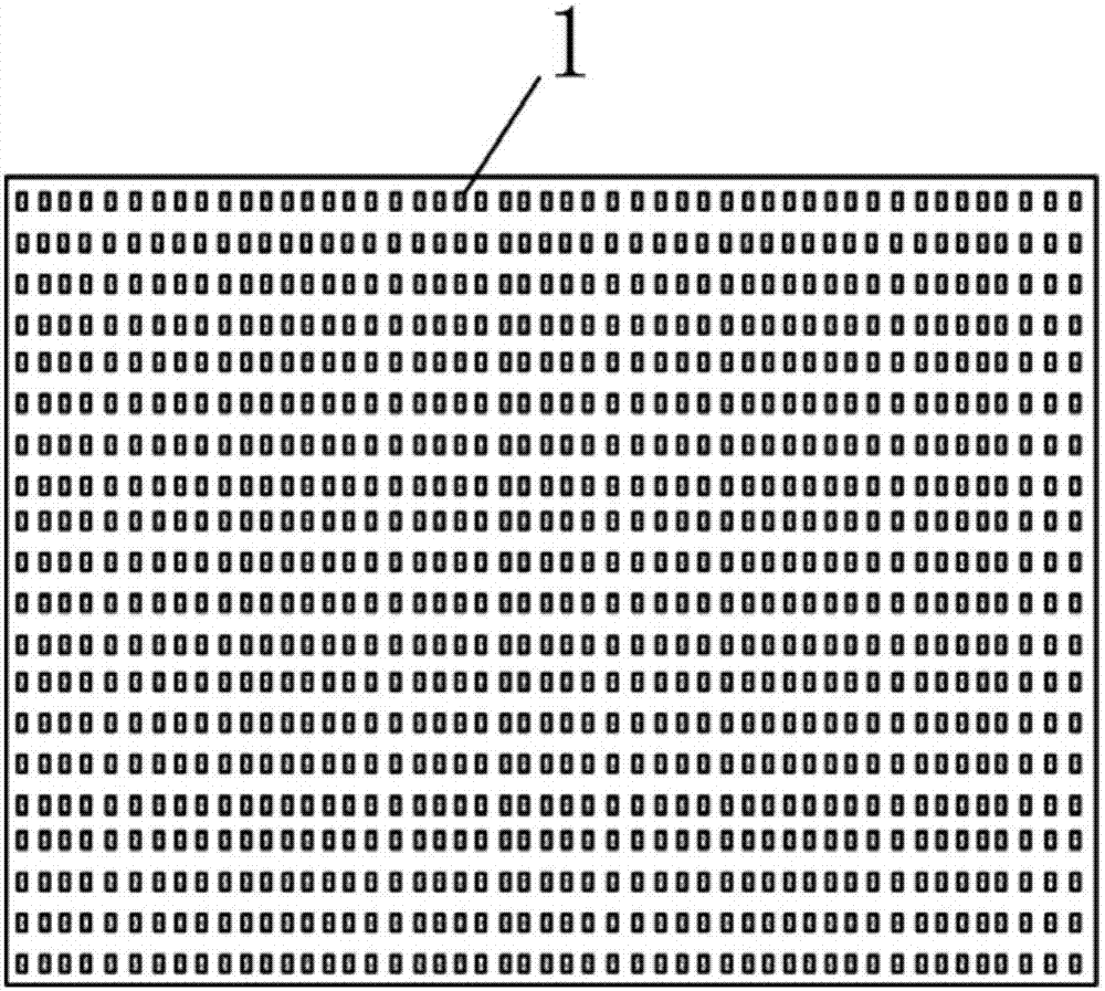
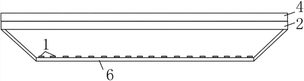
[0052] Such as figure 2 As shown, the backlight unit includes a substrate 6 (with an area of 70cm*40cm), a wavelength conversion film 4, and a cup body; the cup body is formed by extending the edge of the substrate 6 toward the direction of the wavelength conversion film 4, and has an opening. The section is an isosceles inverted trapezoid (base angle 135 degrees), the cup has an opening, side walls and a substrate 6, and the side walls of the cup and the inner surface of the substrate 6 are provided with a reflective film ( figure 2 Not shown in ) substrate 6 has a plurality of groove portions ( figure 2 not shown), the backlight unit also includes a micro LED chip array, the micro LED chip array such as figure 1 as shown ( figure 1 It is only a schematic diagram, and the actual number of micro-LED chips is not shown), the micro-LED chip array includes a plurality of micro-LED chips 1 arranged in a matrix, and the micro-LED chip array includes 2660 rows*7000 micro-LED ...
Embodiment 2
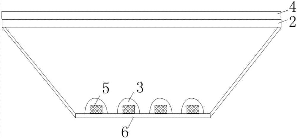
[0055] Such as Figure 4 As shown, the backlight unit includes a substrate 6 (with an area of 15cm*8cm), a wavelength conversion film 4, and the substrate 6 has a plurality of grooves ( Figure 4 not shown), the backlight unit also includes a micro LED chip array, the micro LED chip array such as figure 1 as shown ( figure 1 It is only a schematic diagram, and the actual number of micro-LED chips is not shown), the micro-LED chip array includes a plurality of micro-LED chips 1 arranged in a matrix, and the micro-LED chip array includes 1000 rows*800 micro-LED chips, in the form of a cuboid shape, its length*width*height is 0.05mm*0.1mm*0.05mm, the luminous wavelength range of the micro LED chip 1 is 440-465nm; the distance between each micro LED chip 1 in the length and width direction is 0.05mm, And it has an independent control circuit; the distribution density of micro LED chips 1 is 6666 per square centimeter, and they are embedded in the groove part of the substrate. ...
Embodiment 3
[0058] The micro-LED chip array includes 250 rows*266 columns of micro-LED chips 1, which are in the shape of a cuboid, and its length*width*height is 0.1mm*0.4mm*0.1mm. The distribution density of chip 1 is 554 pieces / square centimeter, and the others are the same as in embodiment 2.
PUM
| Property | Measurement | Unit |
|---|---|---|
| area | aaaaa | aaaaa |
| thickness | aaaaa | aaaaa |
| thickness | aaaaa | aaaaa |
Abstract
Description
Claims
Application Information