Organic EL display device and liquid crystal display device
A liquid crystal display device and display device technology, applied in lighting devices, liquid crystal materials, instruments, etc., can solve problems such as wiring and component damage
- Summary
- Abstract
- Description
- Claims
- Application Information
AI Technical Summary
Problems solved by technology
Method used
Image
Examples
Embodiment 1
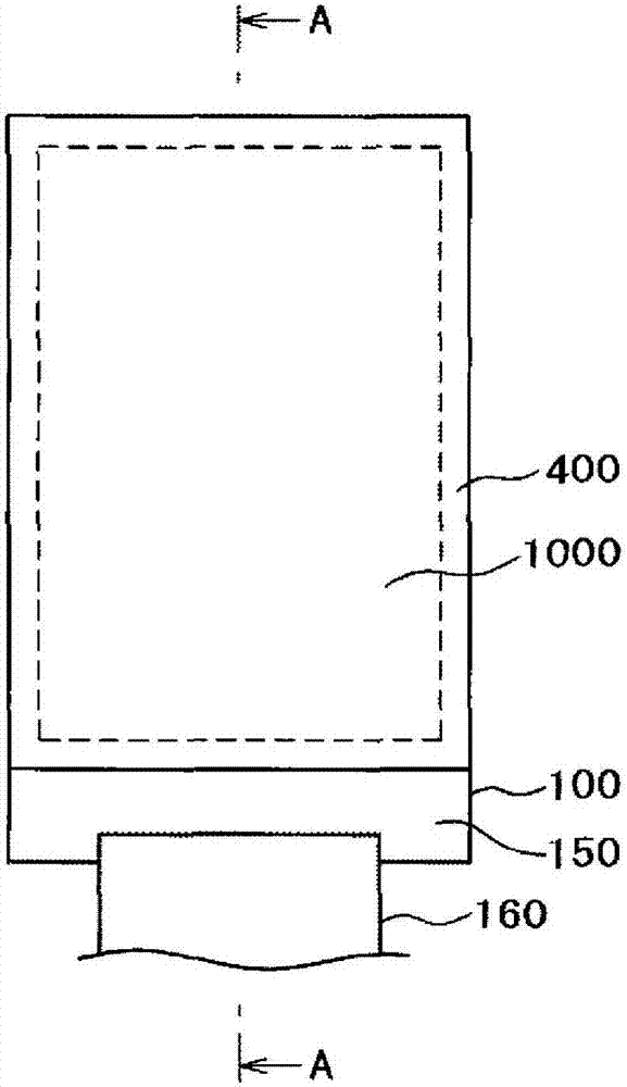
[0045] figure 1 It is a plan view showing an example of an organic EL display device to which the present invention is applied. The organic EL display device of the present invention is a flexibly bendable display device. Since an organic EL display device does not require a backlight, it is advantageous for a flexible display device. figure 1 In this example, the organic EL display device has a display region 1000 and a terminal portion 150, and a polarizer 400 for preventing reflection is attached to the display region 1000. A flexible wiring board 160 for supplying power and signals to the organic EL display device is connected to the terminal portion 150 .
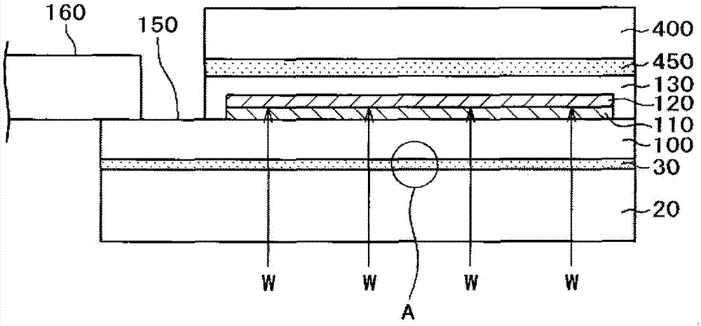
[0046] figure 2 as a comparative example figure 1 A-A sectional view of . An array layer 110 including TFT (Thin Film Transistor, Thin Film Transistor), image signal lines, scanning lines, power supply lines, etc. is formed on the resin substrate 100 . Also in the resin substrate 100, since the polyimide substra...
Embodiment 2
[0072] An organic EL display device is formed by disposing an organic EL material that emits light of different colors for each pixel in the organic EL layer, and forming a color image by using a color filter to emit white light in the organic EL layer. When using a color filter, the counter substrate on which the color filter is formed is arranged on the upper side than the organic EL layer.
[0073] Figure 13 for this example. Figure 13 , until the protective film 130 is formed so as to cover the organic EL layer 120, the same as that of Example 1 Figure 5 same. Figure 13 In this case, in order to attach the opposing substrate 200, a sealing material 210 is formed around the protective layer 130, and an ultraviolet curable resin 220 as an adhesive material is applied inside. The sealing material 210 is provided so that the liquid ultraviolet curable resin 220 does not flow to the outside. The sealing material 210 is obtained by applying and curing epoxy resin, acryli...
Embodiment 3
[0081] Embodiment 1 and Embodiment 2 are examples in which the array layer 110 and the organic EL layer 120 are formed on the polyimide substrate 100 . This embodiment is an example in which the array layer 110 and the organic EL layer 120 are directly formed on the glass substrate 10 without using the polyimide substrate 100 . Figure 15 To illustrate the cross-sectional view of this embodiment.
[0082] Figure 15 Among them, an array layer 110 and an organic EL layer 120 are formed on a glass substrate 10 . Other constitution and embodiment 2 Figure 13 same. express Figure 15 The portion shown in D of the bonding portion between the counter substrate 200 and the upper polarizer 410 is the same as that described in Example 2. Figure 14 same. In addition, the part E showing the bonded part between the glass substrate 10 and the support substrate 20 is the same as that described in Example 1. Figure 7 same.
[0083] It should be noted that since the visibility of t...
PUM
| Property | Measurement | Unit |
|---|---|---|
| radius | aaaaa | aaaaa |
| radius | aaaaa | aaaaa |
Abstract
Description
Claims
Application Information


