
PCB (printed circuit board) matrix fuse and manufacturing method thereof

A manufacturing method and technology of fuses, which are applied in the manufacture of fuses, emergency protection devices, electrical components, etc., can solve problems such as potential safety hazards, incomplete melting of the melt layer, high voltage, etc., and achieve high surge resistance and improve The effect of breaking capacity and surge resistance

Active Publication Date: 2017-12-12
NANJING SART SCI & TECH DEV
View PDF6 Cites 10 Cited by
  • Summary
  • Abstract
  • Description
  • Claims
  • Application Information

AI Technical Summary

Problems solved by technology

However, during the fusing test and breaking test, the melt layer of some PCB fuse products is not completely fused, and the temperature of the remaining melt layer continues to rise under the action of high current and high voltage. When the temperature exceeds 300 ° C, The PCB board turns black or even burns, causing the PCB board fuse to not withstand higher voltage
And the fuse with the PCB board as the base is easier to burn. Due to structural limitations, the problem that the breaking capacity and anti-surge capability of the fuse cannot be improved at the same time while reducing the size is more prominent.
Therefore, small fuses based on PCB boards can only be used in the low-voltage DC field at present, and this type of fuses often fail to withstand frequent surge impacts, resulting in potential safety hazards

Method used


Image

  • PCB (printed circuit board) matrix fuse and manufacturing method thereof
  • PCB (printed circuit board) matrix fuse and manufacturing method thereof
  • PCB (printed circuit board) matrix fuse and manufacturing method thereof

Examples


Embodiment Construction

[0047] The implementation modes of the present invention will be described in further detail below in conjunction with the accompanying drawings.

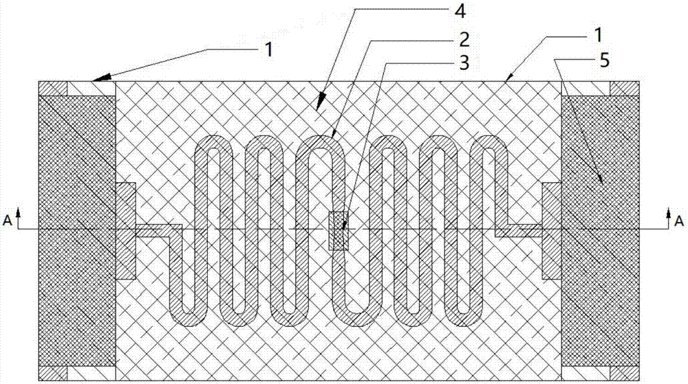
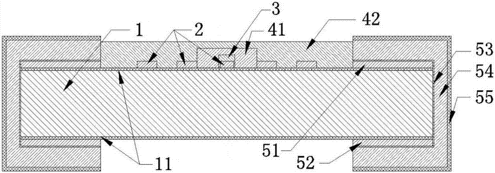
[0048] like Figure 1-2 As shown, a PCB base fuse includes a PCB substrate 1, a melt layer 2 and two terminal electrodes 5, the two terminal electrodes 5 are respectively coated on both ends of the PCB substrate 1, and the melt layer 2 is arranged on the PCB substrate 1 and both ends of the melt layer 2 are respectively connected to two terminal electrodes 5; the central part of the melt layer 2 is also coated with a layer of flux 3, making it an easy-to-fusible effect point, and the flux 3 is covered with a protective layer 4 , and the protective layer 4 completely covers the flux 3 .

[0049] like image 3 As shown, the PCB substrate 1 is also attached with a substrate coating layer 11 at least on the upper surface. The substrate coating layer 11 is made of flame-retardant arc-extinguishing glue and completely covers the upper ...


PUM


Abstract

The invention discloses a PCB (printed circuit board) matrix fuse and a manufacturing method thereof. A PCB substrate is used as a matrix, and is wrapped by flame-retardant arc-extinguishing glue; an effect point part of a melt layer on the upper surface of the PCB substrate is wrapped by a melting supporter; the melting supporter is wrapped by an arc extinguishing protection layer prepared from the flame-retardant arc-extinguishing glue, so that the effect point part, which is easy to fuse, on the melt layer is completely wrapped in the flame-retardant arc-extinguishing glue, and the flame-retardant arc-extinguishing glue is provided with an arc extinguishing layer of a three-dimensional elastic structure and a nanofiller; in case of high current and high voltage in the fuse, a breaking arc generates plasmas which are outwards splashed; the arc extinguishing layer can absorb a large amount of heat and bear energy impact of the plasmas; the nanofiller absorbs a large amount of heat and is partially decomposed, thus generating flame-retardant arc-extinguishing gas which accelerates attenuation of short circuit current to finally extinguish the arc; the breaking capacity is improved, and the surge resisting capacity is also improved. The manufacturing method is mature in process; for a small-sized fuse with high surge resistance and high breaking capacity, the manufacturing method is relatively low in cost.

Description

technical field [0001] The invention relates to a fuse, in particular to a fuse structure for overcurrent and overvoltage protection based on a PCB substrate and a manufacturing method thereof. Background technique [0002] With the development of the electronic industry, the requirements for miniaturization and integration of components in the field of electronic products are getting higher and higher, and the volume of chip protection components is also greatly reduced. However, while reducing the volume of the chip protection element, there is currently no effective solution that can simultaneously improve its breaking performance and anti-surge capability. In particular, chip fuses with a width of less than 6.5mm cannot withstand 220V or higher voltages, and in long-term use, the protection components are also difficult to withstand surges such as frequent switching and indirect lightning, and it is difficult to maintain Long-term stable and effective performance. [0...

Claims


Application Information

Patent Timeline
IPC IPC(8): H01H85/02H01H85/041H01H69/02
CPCH01H69/022H01H85/0241H01H85/0411H01H2085/0275H01H2085/0412
Inventor 南式荣陈兴
Owner NANJING SART SCI & TECH DEV
Learn More