An IGBT structure with an inverted stand surface and a method for manufacturing the same

A fabrication method and substrate surface technology, which can be used in the manufacture of semiconductor/solid-state devices, electrical components, circuits, etc., can solve the problem of inability to maintain the threshold voltage of the gate set parasitic capacitance, and achieve the goal of maintaining the threshold voltage unchanged and reducing the gate voltage. The effect of collecting parasitic capacitance and reducing electromagnetic interference

Inactive Publication Date: 2017-12-22
ZHUZHOU CRRC TIMES SEMICON CO LTD
View PDF3 Cites 0 Cited by
  • Summary
  • Abstract
  • Description
  • Claims
  • Application Information

AI Technical Summary

Problems solved by technology

[0003] The invention provides an inverted mesa gate IGBT structure and its manufacturing method, which are used to solve the technical problem in the prior art that the threshold voltage cannot be kept constant while reducing the parasitic capacitance of the gate set

Method used


Image

  • An IGBT structure with an inverted stand surface and a method for manufacturing the same
  • An IGBT structure with an inverted stand surface and a method for manufacturing the same
  • An IGBT structure with an inverted stand surface and a method for manufacturing the same

Examples


Embodiment 1

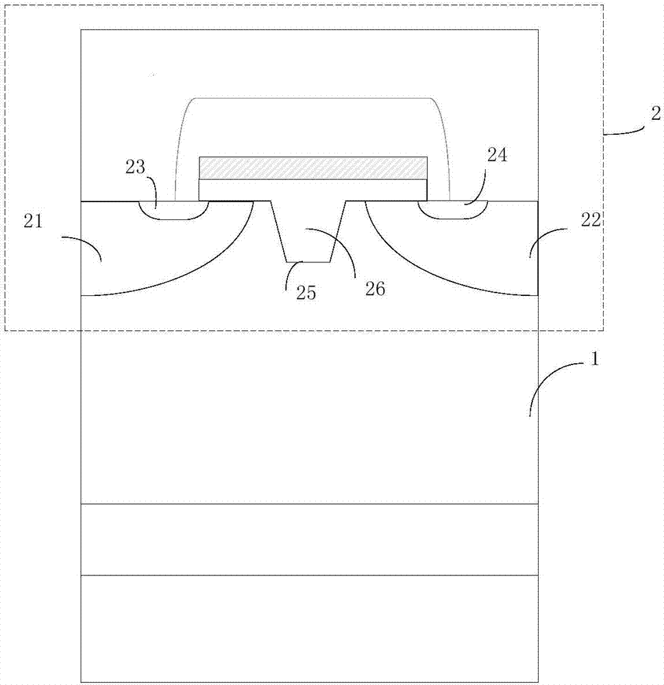
[0039] figure 2 A schematic structural diagram of an inverted mesa gate IGBT structure provided for Embodiment 1 of the present invention; figure 2 As shown, this embodiment provides an inverted mesa gate IGBT structure, including:

[0040] The semiconductor substrate 1 and the cellular region 2; the cellular region 2 includes a first base region 21 located in the surface of the semiconductor substrate 1, a second base region 22, a first source region 23 located in the first base region 21, and a first source region located in the surface of the semiconductor substrate 1. The second source region 24 in the second base region 22 and the inverted mesa 25 between the first base region 21 and the second base region 22, the inverted mesa 25 is a structure with a wide top and a narrow bottom, and the lower part of the inverted mesa 25 is located on the semiconductor substrate 1, the upper part is flush with the surface of the semiconductor substrate 1, the surface of the semicond...

Embodiment 2

[0046] This embodiment is a supplementary description based on the above embodiments.

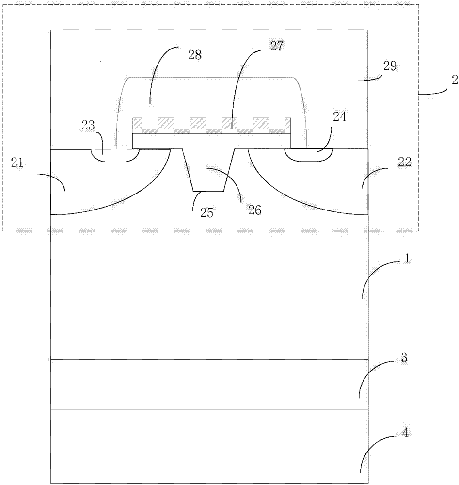
[0047] image 3 A schematic structural diagram of an inverted mesa gate IGBT structure provided for Embodiment 1 of the present invention; image 3 As shown, the cell region 2 further includes a polysilicon layer 27 covering the oxide layer 26 .

[0048] Further, the cell region 2 also includes a passivation layer 28 and a first metal layer 29, wherein the passivation layer 28 covers the polysilicon layer 27, part of the first source region 23 and part of the second source region 24, and the first metal layer 29 Covering the passivation layer 28 , part of the first source region 23 , part of the second source region 24 , part of the first base region 21 and part of the second base region 22 .

[0049] Specifically, the passivation layer 28 is used to separate the first metal layer 29 from the oxide layer 26 and the polysilicon layer 27, and the first metal layer 29 is preferably an alumin...

Embodiment 3

[0056] The manufacturing method of the inverted mesa gate IGBT provided in this embodiment is used to manufacture the inverted mesa gate IGBT structure in the first embodiment above.

[0057] Figure 4 A schematic flow chart of the manufacturing method of the inverted mesa gate IGBT provided in Embodiment 3 of the present invention; as Figure 4 As shown; this embodiment provides a method for manufacturing an inverted mesa gate IGBT, including:

[0058] Step 101, forming an inverted mesa structure in the surface of the semiconductor substrate, the inverted mesa structure is filled with an oxide layer, wherein the inverted mesa structure is wide at the top and narrow at the bottom, the lower part of the inverted mesa is located in the semiconductor substrate, and the upper part is flush with the surface of the semiconductor substrate together.

[0059] The structure formed in this step is as Figure 5 As shown, numeral 400 is a semiconductor substrate, and numeral 401 is an ...


PUM


Abstract

The invention provides an IGBT structure with an inverted stand surface. The IGBT structure comprises a semiconductor substrate and a cell region; the cell region includes a first base region and a second base region located in the surface of the semiconductor substrate, a first source region located in the first base region, a second source region located in the second base region, and an inverted table surface located between the first base region and the second base region; the inverted table surface has a structure with a wide upper portion and a narrow lower portion; the lower portion of the inverted table surface is located in the semiconductor substrate and the upper portion is flush with the surface of the semiconductor substrate; the surface of the semiconductor surface is covered with an oxidation layer between part of the first source region and part of the second source region; the inverted stand surface is filled with an oxidation layer. The IGBT structure has the advantage that on the premise that the threshold voltage is kept the same by maintaining the thickness of the oxidation layer above a channel and increasing the thickness of the oxidation layer between the first base region and the second base region, gate stray capacitance is greatly reduced to reduce electromagnetic interference in an on/off process of an IGBT.

Description

technical field [0001] The invention relates to the field of semiconductor devices, in particular to an inverted mesa gate IGBT structure and a manufacturing method thereof. Background technique [0002] Insulated Gate Bipolar Transistor (IGBT) cells have gate set parasitic capacitance, which will make the IGBT susceptible to electromagnetic interference during the switching process, causing the gate voltage to oscillate, thereby deteriorating the switching performance of the IGBT. Difference. The typical structure of an ordinary IGBT cell is as follows figure 1 As shown, the uniform thickness of its entire oxide layer a is t. The oxide layer a can be divided into two parts. The thickness of the oxide layer b above the channel determines the threshold voltage of the IGBT, while the thickness of the oxide layer c between the two bases determines the parasitic capacitance of the gate set. Due to the limitation of the threshold voltage of the IGBT, the value of t can only be...

Claims


Application Information

Patent Timeline
Patent Type & Authority Applications(China)
IPC IPC(8): H01L29/739H01L29/06H01L21/331
Inventor 刘国友朱利恒覃荣震罗海辉黄建伟戴小平
Owner ZHUZHOU CRRC TIMES SEMICON CO LTD
Why Eureka
Try Eureka