High-voltage transistor and manufacturing method thereof

A technology of high-voltage transistors and manufacturing methods, applied in semiconductor/solid-state device manufacturing, semiconductor devices, electrical components, etc., can solve the problems of increasing the thickness of the gate oxide layer, reducing the saturation current, and unfavorable conductive channel formation. The effect of increasing the breakdown voltage

Inactive Publication Date: 2010-06-02
GRACE SEMICON MFG CORP
View PDF0 Cites 5 Cited by
  • Summary
  • Abstract
  • Description
  • Claims
  • Application Information

AI Technical Summary

Problems solved by technology

However, in such figure 1 In the structure of the high-voltage transistor shown, since the oxide layer 13 is not only an oxide layer between the drain terminal and the gate 14, but also a gate oxide layer at the same time, the thickness of the oxide layer between the drain terminal and the gate 14 is increased, It will inevitably lead to an increase in the thickness of the gate oxide layer at the same time, which is not conducive to the formation of a conductive channel, thereby reducing the saturation current

Method used


Image

  • High-voltage transistor and manufacturing method thereof
  • High-voltage transistor and manufacturing method thereof
  • High-voltage transistor and manufacturing method thereof

Examples


Embodiment Construction

[0024] In order to make the purpose and features of the present invention more comprehensible, the specific implementation manners of the present invention will be further described below in conjunction with the accompanying drawings.

[0025] The core idea of ​​the present invention is that the first oxide layer and the second oxide layer can have different Thickness, while increasing the thickness of the first oxide layer to increase the breakdown voltage, keep the thickness of the second oxide layer constant so as not to affect the saturation current.

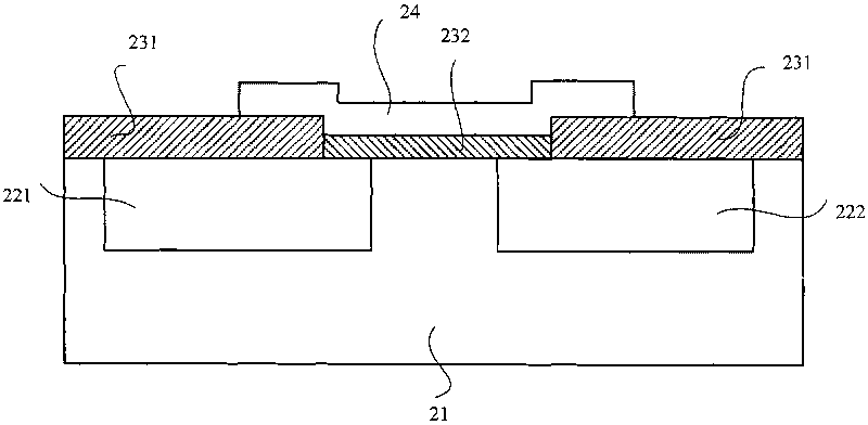
[0026] see figure 2 , figure 2 It is a schematic structural diagram of a high-voltage transistor according to the present invention. figure 2 Among them, the high voltage transistor includes: a high voltage well region 21; a source drift region 221 and a drain drift region 222, both formed in the high voltage well region 21; a first oxide layer 231 formed in the source drift region 221 and on the drain drift region 222...


PUM


Abstract

The invention discloses a high-voltage transistor and a manufacturing method thereof. The high-voltage transistor is formed by a first oxidizing layer between a drain terminal and a grid electrode and a second oxidizing layer used as a grid oxidizing layer in different steps. The first oxidizing layer and the second oxidizing layer can have different thicknesses, then the thickness of the second oxidizing layer can be maintained without influencing the saturation current when he thickness of the first oxidizing layer is increased so as to enhance a breakdown voltage, and then the breakdown voltage is enhanced on the premise of not influencing the saturation current. In addition, the manufacturing method of the high voltage transistor is compatible with traditional manufacturing process of the high-voltage transistor, and does not need additional mask.

Description

technical field [0001] The invention relates to the technical field of silicon semiconductor devices, in particular to a high-voltage transistor and a manufacturing method thereof. Background technique [0002] At present, the application of high-voltage devices in integrated circuit products is becoming more and more extensive, and their influence and attention are getting higher and higher. The normal operating voltage of high-voltage devices is greater than 8V, and the normal operating voltage of ordinary low-voltage devices is not greater than 5V. There are many kinds of high-voltage devices, and the structure of a common high-voltage transistor is as follows figure 1 shown. figure 1 Among them, the high-voltage transistor includes a high-voltage well region 11; a source drift region 121 and a drain drift region 122 are both formed in the high-voltage well region 11; an oxide layer 13 is formed on the high-voltage well region 11; a gate 14 , formed on the oxide layer ...

Claims


Application Information

Patent Timeline
Patent Type & Authority Applications(China)
IPC IPC(8): H01L29/78H01L29/06H01L21/336H01L21/28
Inventor 唐树澍
Owner GRACE SEMICON MFG CORP
Why Eureka
Try Eureka