Holographic laser film coated non-contact IC (Integrated Circuit) card

A non-contact, film bonding technology, applied in the direction of cards, synthetic resin layered products, record carriers used by machines, etc., can solve the problems of increased manpower and material resources required for production, increased scrap rate, and high production costs, and achieve enhanced Surface effect performance, low frequency loss, and long service life

Inactive Publication Date: 2018-01-02
深圳市千丰彩智能科技发展有限公司
View PDF8 Cites 3 Cited by
  • Summary
  • Abstract
  • Description
  • Claims
  • Application Information

AI Technical Summary

Problems solved by technology

In this way, each batch of orders for related laser materials has to be made separately on the chip layer, and it takes 5-10 seconds / round longer than normal, resulting in increased manpower and material resources required for production, resulting in high production costs, low efficiency, and increased scrap rates.

Method used


Image

  • Holographic laser film coated non-contact IC (Integrated Circuit) card
  • Holographic laser film coated non-contact IC (Integrated Circuit) card
  • Holographic laser film coated non-contact IC (Integrated Circuit) card

Examples


Embodiment 1

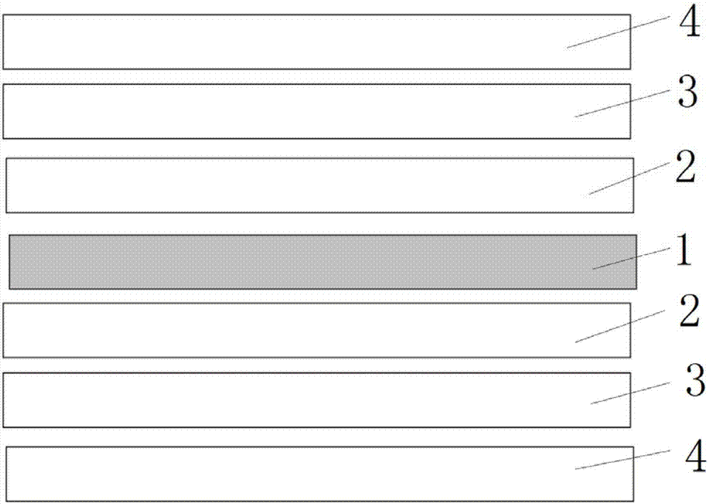
[0022] refer to figure 1 , figure 2 As shown, a non-contact IC card bonded with a holographic laser film includes an IC chip 1 and a card structure, the IC chip 1 is arranged in the card structure, and the card structure includes an upper side card structure, a lower side Card structure, the upper side card structure includes a holographic PET / PVC laser plastic layer group 2, a printing layer 3, a PET / PVC film layer 4 sequentially arranged on the IC chip 1 from the inside to the outside, and the holographic PET The / PVC laser plastic layer group 2 is used to realize functions such as holographic pattern and laser pattern, the printing layer 3 is used for pattern printing, and the PET / PVC film layer 4 is used to protect the inner layer.

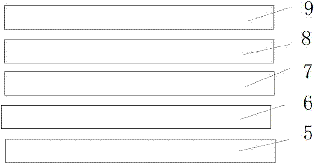
[0023] The holographic PET / PVC laser plastic layer group 2 includes a PET / PVC plastic layer 5, a glue layer 6, a combined layer 7, a metallized layer / nano new material layer 8, and a PET / PVC base film layer arranged in sequence from the insi...

Embodiment 2

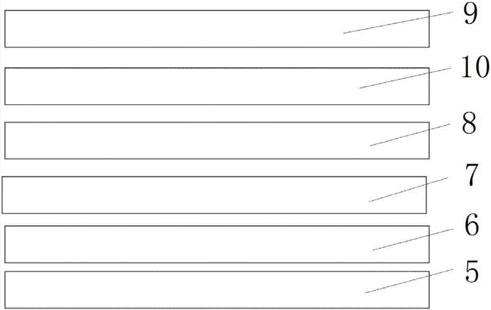
[0029] refer to Figure 4 As shown, the difference between this embodiment and Embodiment 1 is that the lower card structure includes a PET / PVC plastic layer 5, a printing layer 3, a PET / PVC plastic layer 5, a printing layer 3, and a PET / PVC layer arranged on the IC chip 1 from the inside to the outside. Thin-film layer 4, that is, the lower side of the IC card does not have holographic or laser effects.

[0030] Under the same conditions, after testing, when the metal-plated layer / nano new material layer is an aluminum-plated layer, the layer thickness of the existing holographic process Compared with the effect that the maximum distance that can be read by single-sided use is 35-40mm, and the maximum distance that can be read by double-sided use is 25-30mm, using the IC card of the present invention, the single-sided one in Embodiment 2 has holographic and laser effects. The maximum reading distance is 40-45mm, the reading distance is increased by 5±2mm, and the frequency ...


PUM


Abstract

The invention discloses a holographic laser film coated non-contact IC (Integrated Circuit) card which comprises an IC chip and a card structure, wherein the IC chip is arranged inside the carbon structure; the card structure comprises an upper card structure and a lower card structure; the upper card structure comprises a holographic PET / PVC (Polyethylene Terephthalate / Polyvinyl Chloride) laser plastic layer group, a printed layer and a PET / PVC film layer; the PET / PVC laser plastic layer group is used for bringing functions of holographic patterns and laser patterns into play; the printed layer is configured for pattern printing; and the PET / PVC film layer is used for protecting inner layers. The holographic laser film coated non-contact IC card disclosed by the invention solves the problem that a chip is too small in emission frequency after a holographic laser film is pasted to a PVC card, is capable of improving the surface effect properties of printed patterns of the card making industry, has the characteristics of being large in reading distance, small in frequency consumption, possible in in-batch production, good in surface effect, long in service life, good in anti-fake property and the like, and has wide application prospects in the field of various IC cards.

Description

technical field [0001] The invention relates to the technical field of IC card making, in particular to a non-contact IC card bonded with a holographic laser film. Background technique [0002] IC card is to embed a microelectronic chip into the card base conforming to the ISO 7816 standard, and make it into a card form. According to the communication interface, the IC card can be divided into contact IC card, non-contact IC card and dual interface card. Non-contact IC card, also known as radio frequency card, is composed of IC chip and induction antenna, and is packaged in a standard PVC card. The chip and antenna have no exposed parts, and successfully solve the problem of passive (no power supply in the card) and contact-free This problem is a major breakthrough in the field of electronic devices. It has the advantages of high reliability, anti-collision (automatic resolution capability), convenient operation, wide application range, and good encryption performance. It is...

Claims


Application Information

Patent Timeline
Patent Type & Authority Applications(China)
IPC IPC(8): G06K19/02G06K19/077
CPCG06K19/06065G06K19/0723G06K19/07722B32B27/06B32B2307/75B32B2425/00B32B2307/402B32B27/304B32B7/12B32B2255/205B32B2250/05B32B2307/416B32B2457/00B32B2307/202B32B27/36B32B2307/412G06K19/07749
Inventor 许贵贤洪宝丽
Owner 深圳市千丰彩智能科技发展有限公司
Why Eureka
Try Eureka